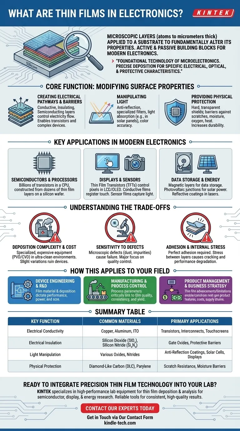
At its core, a thin film in electronics is a microscopic layer of material, often just a few atoms to a few micrometers thick, intentionally applied to a surface (called a substrate) to fundamentally alter its properties. These engineered layers are not merely coatings; they are the active and passive building blocks that enable the function of virtually every modern electronic component, from the transistors in a CPU to the pixels on a display.
Thin films are the foundational technology of microelectronics. By precisely depositing ultra-thin layers of different materials, we can create specific electrical, optical, and protective characteristics on a surface that are impossible to achieve with the bulk material alone.
The Core Function: Modifying a Surface's Properties
The entire purpose of a thin film is to give a material's surface new capabilities. A simple piece of silicon or glass is inert, but by adding a sequence of thin films, we can transform it into a complex electronic device.
Creating Electrical Pathways and Barriers
The most critical function of thin films in electronics is controlling the flow of electricity. Layers are designed to be either conductive (letting electricity pass, like microscopic wires), insulating (blocking electricity), or semiconducting (acting as a switch). Stacking these layers in precise patterns is how a transistor, the fundamental switch in all modern computing, is built.
Manipulating Light
Thin films are essential for managing how devices interact with light. This includes anti-reflection films on smartphone screens and camera lenses that improve clarity, as well as specialized filter films on image sensors that help capture color accurately. In solar panels (photovoltaic devices), specific thin films are designed to maximize light absorption and efficiently convert it into electricity.
Providing Physical Protection
Beyond active electrical or optical roles, thin films serve as crucial protective barriers. They can form a hard, transparent shield over a display to resist scratches or create an impermeable barrier to protect sensitive internal components from moisture, oxygen, and heat. This dramatically increases the durability and lifespan of a device.
Key Applications in Modern Electronics
You interact with thin film technology constantly. It is not a niche component but the bedrock of the entire electronics industry.
In Semiconductors and Processors
An integrated circuit (IC), or "chip," is the most dramatic example of thin film engineering. A modern CPU contains billions of transistors, each constructed from a complex stack of dozens of different thin film layers deposited onto a silicon wafer. The performance of the chip is a direct result of the precision, purity, and properties of these films.
In Displays and Sensors
Modern high-resolution displays (LCD and OLED) rely on a grid of Thin Film Transistors (TFTs) to control each individual pixel. Similarly, the conductive films in a touchscreen register your touch, and the layered films in a digital camera sensor capture light to form an image.
In Data Storage and Energy
Thin films are used to create the magnetic layers on a hard disk drive's platters where data is stored. In solar cells, a sequence of thin films forms the photovoltaic junction that generates power. They are also used as reflective coatings in lasers and protective layers in optical discs.
Understanding the Trade-offs
While powerful, thin film technology presents significant engineering challenges that define the limits and costs of modern electronics.
Deposition Complexity and Cost
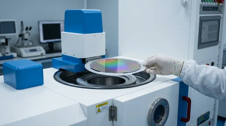
Applying a perfectly uniform film that is mere nanometers thick requires highly specialized and expensive equipment operating in an ultra-clean environment. The methods used, such as Physical Vapor Deposition (PVD) or Chemical Vapor Deposition (CVD), are complex processes where slight variations can ruin the final device.
Sensitivity to Defects
Because these layers are so thin, even a microscopic defect—a single speck of dust or a tiny impurity in the material—can cause a component to fail. This sensitivity is a primary driver of manufacturing cost and a major focus of quality control in the semiconductor industry.
Adhesion and Internal Stress
The thin film must adhere perfectly to the substrate below it. Any failure in adhesion can lead to peeling and device failure. Furthermore, stress can build up between layers due to differences in their physical properties, which can cause cracking or performance degradation over the device's lifetime.
How This Applies to Your Field
Your approach to thin films will depend on your specific role, but the underlying principles are universal.
- If your primary focus is device engineering or R&D: Your key takeaway is that the choice of film material and its deposition method directly dictates component performance, power consumption, and physical size.
- If your primary focus is manufacturing or process control: Your key takeaway is the critical link between process parameters (temperature, pressure, etc.) and the resulting film's quality, consistency, and yield.
- If your primary focus is product management or business strategy: Your key takeaway is that thin film technology advancements (or limitations) are what enable—or constrain—next-generation product features, costs, and supply chains.
By understanding these microscopic layers, you can appreciate that modern electronics are not just assembled components, but are sculpted from materials at an atomic scale.
Summary Table:
| Key Function | Common Materials | Primary Applications |
|---|---|---|
| Electrical Conductivity | Copper, Aluminum, ITO | Transistors, Interconnects, Touchscreens |
| Electrical Insulation | Silicon Dioxide (SiO₂), Silicon Nitride (Si₃N₄) | Gate Oxides, Protective Barriers |
| Light Manipulation | Various Oxides, Nitrides | Anti-Reflection Coatings, Solar Cells, Displays |
| Physical Protection | Diamond-Like Carbon (DLC), Parylene | Scratch Resistance, Moisture Barriers |
Ready to Integrate Precision Thin Film Technology into Your Lab?
Thin films are the foundation of advanced electronics, and the right equipment is critical for R&D, manufacturing, and quality control. KINTEK specializes in high-performance lab equipment for thin film deposition and analysis, serving the precise needs of laboratories in semiconductor, display, and energy research.
We provide the reliable tools you need to achieve consistent, high-quality results. Contact our experts today to discuss how our solutions can accelerate your development and enhance your process yields.
Get in Touch via Our Contact Form
Visual Guide
Related Products
- Aluminized Ceramic Evaporation Boat for Thin Film Deposition
- Tungsten Evaporation Boat for Thin Film Deposition
- Electron Beam Evaporation Coating Oxygen-Free Copper Crucible and Evaporation Boat
- Molybdenum Tungsten Tantalum Evaporation Boat for High Temperature Applications
- Aluminum-Plastic Flexible Packaging Film for Lithium Battery Packaging
People Also Ask
- Why is an alumina boat selected for catalyst precursors? Ensure Sample Purity at 1000 °C
- What are thin films deposited by evaporation? A Guide to High-Purity Coating
- Why are high-purity ceramic boats used for lignin activation? Ensure Purity & Thermal Stability
- What is the chemical method for thin film deposition? Build Films from the Molecular Level Up
- What are the alternatives to sputtering? Choose the Right Thin Film Deposition Method


