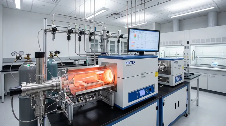
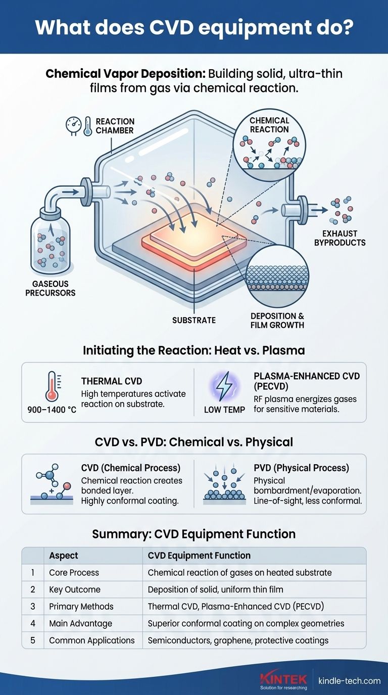
In short, Chemical Vapor Deposition (CVD) equipment is a system that builds a solid, ultra-thin film of material on a surface by using a chemical reaction from a gas. It introduces specific reactive gases, known as precursors, into a controlled chamber. These gases then react or decompose on a heated target object (the substrate), depositing a new, high-purity layer atom by atom.
The core function of CVD equipment is not to simply coat a surface, but to create a precisely controlled chemical reaction in a gaseous state. This reaction's solid byproduct forms a high-performance, uniform film that becomes an integral part of the final object.
The Core Principle: Building Solids from Gases
To understand what CVD equipment does, it's best to break the process down into its fundamental stages. The entire operation is a carefully orchestrated sequence inside a highly controlled environment.
The Starting Materials: Gaseous Precursors
The raw materials for the film are not solid chunks or liquids but are volatile gases called precursors.
These gases contain the specific atoms (like carbon for graphene or silicon for semiconductors) needed to create the final film. They are mixed with carrier gases and injected into the system.
The Environment: The Reaction Chamber
The entire process takes place inside a sealed reaction chamber.
This chamber allows for the precise control of critical variables like temperature, pressure, and the flow rate of gases, ensuring the chemical reaction happens exactly as intended.
The Foundation: The Substrate
The object being coated is called the substrate. This could be a silicon wafer, a metal foil, or another component.
The substrate is heated to a specific temperature and serves as the surface where the new film will form. In many cases, the substrate's surface also acts as a catalyst, initiating and facilitating the chemical reaction.
The Main Event: The Chemical Reaction
This is the "Chemical" in CVD. As the precursor gases flow over the hot substrate, the energy causes them to react or decompose.
This is a fundamental chemical change where gas molecules break apart and recombine to form a new, solid material.
The Result: Deposition and Film Growth
The solid product of this chemical reaction is deposited onto the substrate's surface, forming a thin, solid film.
This process builds the film layer by layer, resulting in an exceptionally uniform and high-quality coating. The film can be either crystalline (with an ordered atomic structure, like graphene) or amorphous (disordered).
The Cleanup: Exhausting Byproducts
The chemical reaction also creates gaseous byproducts that are not part of the film.
This waste gas is continuously removed from the chamber via a gas flow or vacuum system to prevent contamination and maintain the purity of the deposited layer.
Initiating the Reaction: Heat vs. Plasma
The energy needed to drive the chemical reaction is a critical factor and a key differentiator in CVD systems.
Thermal CVD
This is the most common method, relying on high temperatures (often 900–1400 °C) to provide the necessary activation energy for the precursor gases to react on the substrate.
Plasma-Enhanced CVD (PECVD)
For substrates that cannot withstand high temperatures, plasma is used to energize the precursor gases instead.
An RF (radio frequency) plasma dissociates the gases into reactive ions and radicals at a much lower temperature, allowing for deposition on sensitive materials like plastics.
Understanding the Trade-offs: Chemical vs. Physical Deposition
It's crucial to distinguish CVD from its counterpart, Physical Vapor Deposition (PVD), to understand its unique function.
The Core Distinction
CVD is a chemical process. It creates a film of a new material through a chemical reaction on the substrate's surface. This results in a strong, chemically bonded layer.
PVD is a physical process. It involves physically bombarding, evaporating, or sublimating a solid source material in a vacuum and having it condense on the substrate. No fundamental chemical reaction occurs.
Why Choose CVD?
CVD is often chosen when film quality and uniformity are paramount. Because the precursor is a gas, it can flow into and coat complex, non-line-of-sight geometries with a highly conformal layer, something PVD struggles with. The resulting films are often denser and have superior adhesion.
Making the Right Choice for Your Goal
The type of CVD equipment and process you use depends entirely on the material you are depositing and the substrate you are coating.
- If your primary focus is high-purity, crystalline films on heat-resistant substrates: Traditional Thermal CVD is the established standard for applications in semiconductors or advanced materials like graphene.
- If your primary focus is coating temperature-sensitive materials like polymers or certain electronics: Plasma-Enhanced CVD (PECVD) is the necessary choice, as it achieves high-quality deposition without requiring damagingly high temperatures.
- If your primary focus is creating a very dense, adherent, and uniform coating on a complex shape: CVD is generally superior to line-of-sight physical deposition methods.
Ultimately, CVD equipment provides a powerful and precise method for engineering materials at the atomic level, enabling the creation of advanced films that are fundamental to modern technology.
Summary Table:
| Aspect | CVD Equipment Function |
|---|---|
| Core Process | Chemical reaction of gases on a heated substrate |
| Key Outcome | Deposition of a solid, uniform thin film |
| Primary Methods | Thermal CVD, Plasma-Enhanced CVD (PECVD) |
| Main Advantage | Superior conformal coating on complex geometries |
| Common Applications | Semiconductors, graphene, protective coatings |
Ready to engineer materials at the atomic level? KINTEK specializes in advanced CVD equipment and consumables for laboratories. Whether you need high-purity thermal systems for semiconductor research or low-temperature PECVD for sensitive substrates, our solutions deliver precise, uniform films for your most critical applications. Contact our experts today to discuss how our CVD technology can accelerate your R&D and production.
Visual Guide
Related Products
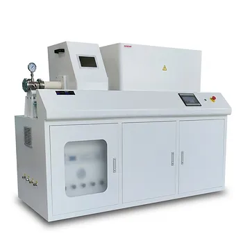
- Chemical Vapor Deposition CVD Equipment System Chamber Slide PECVD Tube Furnace with Liquid Gasifier PECVD Machine
- HFCVD Machine System Equipment for Drawing Die Nano-Diamond Coating
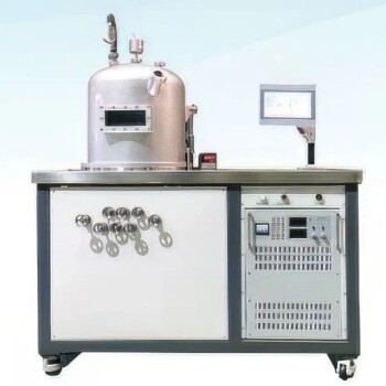
- Multi Heating Zones CVD Tube Furnace Machine Chemical Vapor Deposition Chamber System Equipment
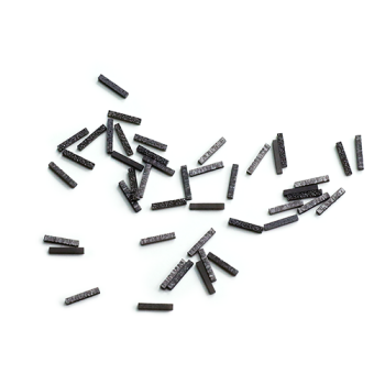
- CVD Diamond Dressing Tools for Precision Applications
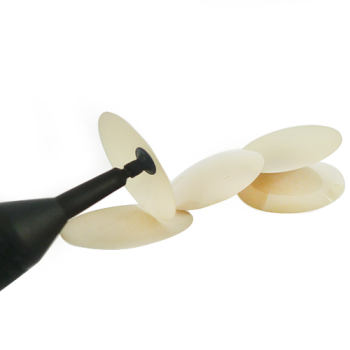
- CVD Diamond Domes for Industrial and Scientific Applications
People Also Ask
- What are the advantages of chemical vapor deposition? Achieve Superior Thin Films for Your Lab
- What are the processes of vapor phase deposition? Understand CVD vs. PVD for Superior Thin Films
- What types of substrates are used in CVD to facilitate graphene films? Optimize Graphene Growth with the Right Catalyst
- How expensive is chemical vapor deposition? Understanding the True Cost of High-Performance Coating
- What happens during deposition chemistry? Building Thin Films from Gaseous Precursors
