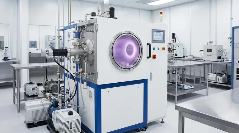
At its core, a sputtering tool is a highly specialized piece of equipment that operates under a high vacuum to deposit exceptionally thin and uniform layers of material onto a surface. This process, known as sputter deposition, is not about melting or evaporating material; instead, it uses a physical mechanism to precisely transfer atoms from a source (the "target") to a destination (the "substrate").
A sputtering tool functions like a subatomic sandblaster. It uses high-energy ions in a vacuum to physically knock atoms off a source material, which then travel and deposit as a highly controlled, ultra-thin film onto another object.
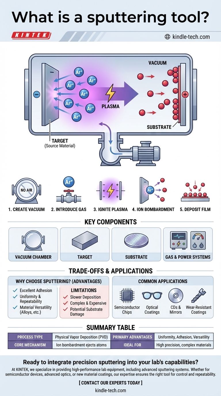
How Sputtering Works: From Plasma to Thin Film
The sputtering process is a type of Physical Vapor Deposition (PVD) that relies on a series of carefully controlled physical steps to build a film, one atom at a time.
Step 1: Creating the Vacuum
The entire process must occur in a high-vacuum chamber. This is non-negotiable, as it removes air and other particles that would otherwise collide with the sputtered atoms and contaminate the final film.
Step 2: Introducing the Sputtering Gas
A small, precisely controlled amount of an inert gas, typically Argon (Ar), is introduced into the vacuum chamber. This gas will become the "blasting media."
Step 3: Igniting the Plasma
A strong electric field is applied within the chamber. The material to be deposited (the target) is given a negative charge (becoming a cathode), while the substrate holder or chamber walls act as the positive charge (anode). This high voltage ignites the Argon gas, stripping electrons from its atoms and creating a visible glow of ionized gas known as a plasma.
Step 4: Ion Bombardment
The positively charged Argon ions (Ar+) within the plasma are now powerfully accelerated toward the negatively charged target. They collide with the target surface with significant kinetic energy.
Step 5: Deposition on the Substrate
This high-energy bombardment physically knocks out, or "sputters," atoms from the target material. These ejected atoms travel through the vacuum and land on the substrate, gradually building up a thin, uniform, and dense film.
Key Components of a Sputtering System
While designs vary, all sputtering tools share several fundamental components that enable this precise process.
The Vacuum Chamber
This is the sealed enclosure where the deposition takes place. It's connected to a series of powerful pumps capable of removing nearly all the air to create the necessary high-vacuum environment.
The Target (Source Material)
This is a block or plate made of the material you wish to deposit. It can be a pure metal, an alloy, or even a ceramic compound. The target serves as the source of the coating atoms.
The Substrate
This is the object or wafer that receives the coating. It is carefully positioned inside the chamber to ensure it is coated evenly by the sputtered atoms.
The Gas and Power Systems
A gas handling system controls the precise flow of Argon into the chamber. A high-voltage power supply—either Direct Current (DC) for conductive targets or Radio Frequency (RF) for non-conductive (insulating) targets—provides the energy to create and sustain the plasma.
Understanding the Trade-offs and Applications
Sputtering is chosen for specific reasons and is a cornerstone technology in many advanced industries.
Why Choose Sputtering?
The primary advantage of sputtering is control. It produces films with excellent adhesion to the substrate, exceptional uniformity over large areas, and highly repeatable thickness. It can also be used to deposit complex materials like alloys without altering their chemical composition.
Common Applications
You can find sputtered films everywhere in modern technology. They are used to create the microscopic metal wiring in semiconductor chips, apply anti-reflective coatings on eyeglass lenses, produce the reflective layers on CDs and mirrors, and apply hard, wear-resistant coatings on cutting tools.
Limitations to Consider
Sputtering is generally a slower deposition process compared to alternatives like thermal evaporation. The equipment is also complex and expensive. Furthermore, the high-energy nature of the ion bombardment can sometimes cause damage to very delicate or sensitive substrates.
Making the Right Choice for Your Goal
Understanding the core strengths of sputtering helps clarify its role in manufacturing and research.
- If your primary focus is precision and film quality: Sputtering is the superior choice for creating dense, highly adherent films with excellent thickness control, essential for optics and electronics.
- If your primary focus is material versatility: The ability to deposit alloys, compounds, and insulators (using RF power) makes sputtering more flexible than methods limited to pure, low-melting-point metals.
- If your primary focus is high-speed deposition of simple metals: You might investigate thermal evaporation, which can be a faster and less complex process for certain applications.
Ultimately, the sputtering tool is an indispensable instrument for engineering materials at the atomic scale, enabling the performance of countless high-tech products.
Summary Table:
| Key Aspect | Description |
|---|---|
| Process Type | Physical Vapor Deposition (PVD) |
| Core Mechanism | Ion bombardment of a target material to eject atoms |
| Primary Advantages | Excellent film uniformity, adhesion, and material versatility |
| Common Applications | Semiconductor metallization, optical coatings, wear-resistant layers |
| Ideal For | Applications requiring high precision and complex material deposition |
Ready to integrate precision sputtering into your lab's capabilities?
At KINTEK, we specialize in providing high-performance lab equipment, including advanced sputtering systems, to meet the exacting demands of modern research and development. Whether you are working on semiconductor devices, advanced optics, or new material coatings, our expertise ensures you get the right tool for unparalleled control and repeatability.
Let's discuss how a KINTEK sputtering solution can enhance your thin-film processes. Contact our experts today for a personalized consultation!
Visual Guide
Related Products
- Professional Cutting Tools for Carbon Paper Cloth Diaphragm Copper Aluminum Foil and More
- Three-dimensional electromagnetic sieving instrument
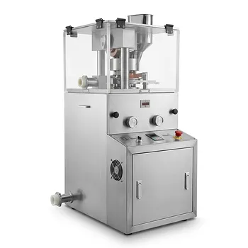
- Single Punch Manual Tablet Press Machine TDP Tablet Punching Machine
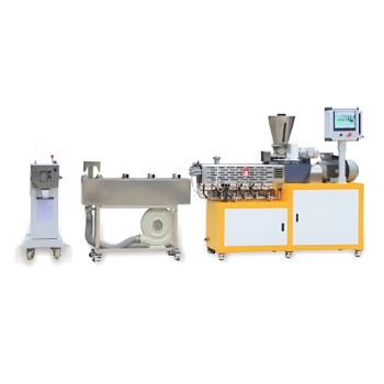
- Twin Screw Extruder Plastic Granulation Machine
- Lab Scale Rotary Single Punch Tablet Press Machine TDP Tablet Punching Machine
People Also Ask
- How can the lifespan of carbon paper be extended? Reinforce Edges with Epoxy for Maximum Durability
- Why is carbon paper placed between the powder and the graphite mold? Protect Your LTPO Electrolytes & Tooling
- How is carbon paper treated for use in fuel cells? The Critical PTFE Coating for Peak Performance
- How should carbon paper be handled during cutting? Prevent Fractures with a Delicate, Precise Approach
- What are the material properties of carbon paper? Unlocking High Conductivity & Porosity for Your Lab