At its core, Chemical Vapor Deposition (CVD) is a sophisticated manufacturing process used to grow a high-purity, solid thin film on a surface, known as a substrate. Inside a reaction chamber, volatile precursor chemicals in a gaseous state are introduced, which then decompose and react on or near the heated substrate to form the desired material layer by layer.
Unlike simply applying a pre-made coating, Chemical Vapor Deposition builds a new solid layer directly onto a surface through a controlled chemical reaction. This atom-by-atom assembly is what makes it indispensable for creating the high-performance materials required in modern electronics and engineering.
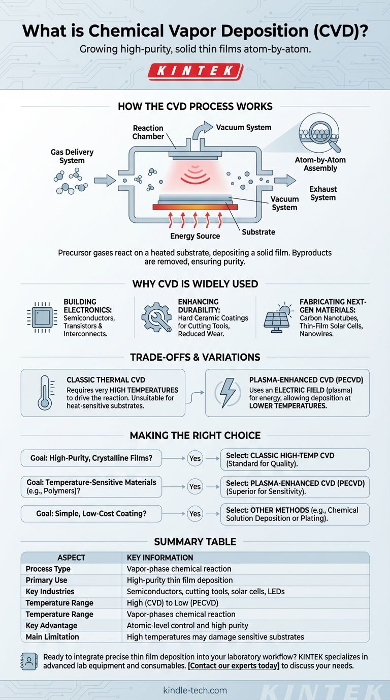
How the CVD Process Works
The CVD process, while complex, can be broken down into a sequence of coordinated steps managed by highly specialized equipment.
The Core Components
A typical CVD system consists of several critical parts working in concert:
- Gas Delivery System: Precisely mixes and introduces precursor gases into the chamber.
- Reaction Chamber: The sealed enclosure where the deposition takes place.
- Energy Source: Heats the substrate to the required reaction temperature.
- Substrate Loading System: Places the workpiece or material to be coated inside the chamber.
- Vacuum System: Removes air and maintains a controlled, low-pressure environment.
- Exhaust System: Safely removes volatile byproducts and unreacted gases after the reaction.
The Chemical Reaction Sequence
The deposition itself follows a clear thermodynamic and chemical pathway.
First, precursor gases are transported into the reaction chamber. The substrate is heated, providing the thermal energy needed to initiate the chemical reaction.
As the gases reach the hot substrate, they react or decompose, and a solid film begins to deposit and grow on the surface. Gaseous byproducts from this reaction are then removed from the chamber by the vacuum and exhaust systems.
The Role of a Controlled Environment
The vacuum is not just for removing air; it is critical for ensuring the purity of the final film. By eliminating unwanted atmospheric gases, the system prevents contamination and allows the desired chemical reaction to proceed cleanly and efficiently.
Why CVD Is So Widely Used
CVD is not just one technique but a foundational platform for fabricating materials with exceptional properties, making it essential across numerous high-tech industries.
Building the Foundation of Electronics
CVD is a cornerstone of the semiconductor industry. It is used to deposit the ultra-pure, crystalline thin films of silicon, silicon nitride, and various metals that form the transistors and interconnects in every microchip.
Enhancing Durability and Performance
In mechanical engineering, CVD is used to apply extremely hard ceramic coatings, like titanium nitride, onto cutting tools and machine parts. This thin film dramatically reduces wear and prevents corrosion, extending the tool's lifespan.
Fabricating Next-Generation Materials
The versatility of CVD allows for the creation of advanced materials that are difficult to produce otherwise. This includes growing carbon nanotubes, depositing photovoltaic materials for thin-film solar cells, and creating GaN nanowires for advanced LEDs and sensors.
Understanding the Trade-offs and Variations
While powerful, CVD is not a universal solution. Understanding its limitations and common variations is key to applying it correctly.
CVD vs. Other Deposition Methods
Chemical deposition is a broad category. Unlike plating, which uses an electrochemical process in a liquid bath, or Chemical Solution Deposition (CSD), which starts with a liquid precursor, CVD's use of gaseous precursors gives it unique control over film purity and structure.
The High-Temperature Requirement
A primary trade-off of classic thermal CVD is the need for very high temperatures to drive the chemical reaction. This makes it unsuitable for depositing films on temperature-sensitive substrates like plastics or certain pre-fabricated electronic components that could be damaged by the heat.
A Key Variation: Plasma-Enhanced CVD (PECVD)
To overcome the temperature limitation, Plasma-Enhanced CVD (PECVD) was developed. In this method, an electric field creates a plasma (an energized gas) inside the chamber.
This plasma provides the energy for the reaction to occur, rather than relying solely on heat. As a result, PECVD can successfully deposit high-quality films at much lower temperatures, expanding its use to a wider range of materials.
Making the Right Choice for Your Goal
Selecting the correct deposition method depends entirely on the material properties you need to achieve and the constraints of your substrate.
- If your primary focus is creating high-purity, crystalline films for semiconductors: Classic, high-temperature CVD is often the standard for achieving the required quality and uniformity.
- If you are working with temperature-sensitive materials like polymers: Plasma-Enhanced CVD (PECVD) is the superior choice to avoid damaging the substrate while still forming a quality film.
- If you need a simple, low-cost coating and atomic-level precision is not critical: Simpler alternatives like chemical solution deposition (CSD) or electroplating may be more practical.
Understanding these fundamental principles allows you to select the precise material fabrication technique for any advanced engineering challenge.
Summary Table:
| Aspect | Key Information |
|---|---|
| Process Type | Vapor-phase chemical reaction |
| Primary Use | High-purity thin film deposition |
| Key Industries | Semiconductors, cutting tools, solar cells, LEDs |
| Temperature Range | High-temperature (CVD) to low-temperature (PECVD) |
| Key Advantage | Atomic-level control and high purity |
| Main Limitation | High temperatures may damage sensitive substrates |
Ready to integrate precise thin film deposition into your laboratory workflow? KINTEK specializes in advanced lab equipment and consumables for cutting-edge material fabrication. Whether you're developing next-generation semiconductors, durable coatings, or novel nanomaterials, our CVD solutions deliver the precision and reliability your research demands. Contact our experts today to discuss how we can support your specific laboratory needs and help you achieve superior material performance.
Visual Guide
Related Products
- Chemical Vapor Deposition CVD Equipment System Chamber Slide PECVD Tube Furnace with Liquid Gasifier PECVD Machine
- Customer Made Versatile CVD Tube Furnace Chemical Vapor Deposition Chamber System Equipment
- Microwave Plasma Chemical Vapor Deposition MPCVD Machine System Reactor for Lab and Diamond Growth
- 915MHz MPCVD Diamond Machine Microwave Plasma Chemical Vapor Deposition System Reactor
- Custom CVD Diamond Coating for Lab Applications
People Also Ask
- What are the advantages of chemical vapor deposition? Achieve Superior Thin Films for Your Lab
- What is plasma enhanced chemical vapor deposition PECVD equipment? A Guide to Low-Temperature Thin Film Deposition
- How are carbon nanotubes grown? Master Scalable Production with Chemical Vapor Deposition
- How expensive is chemical vapor deposition? Understanding the True Cost of High-Performance Coating
- What types of substrates are used in CVD to facilitate graphene films? Optimize Graphene Growth with the Right Catalyst


