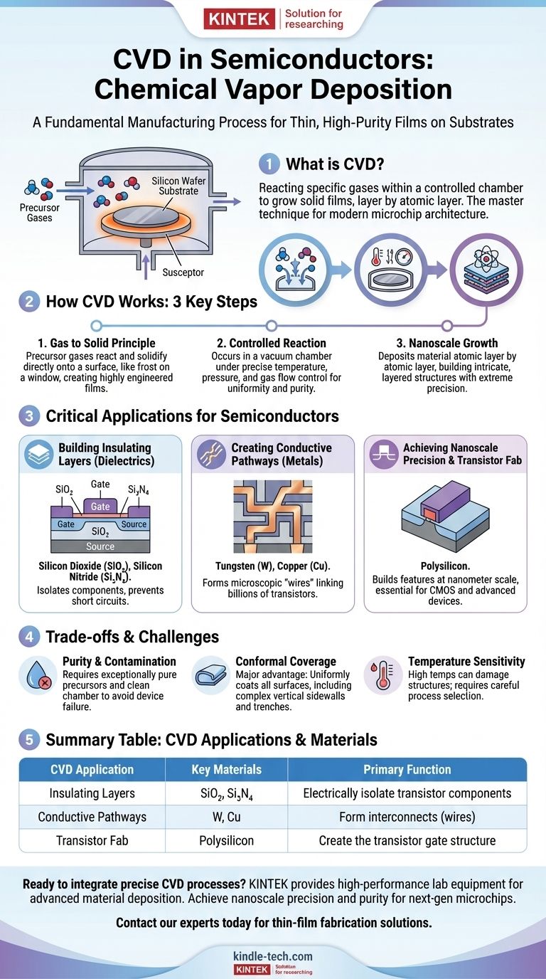
In the context of semiconductors, CVD stands for Chemical Vapor Deposition. It is a fundamental manufacturing process used to grow extremely thin, high-purity solid films on a substrate, such as a silicon wafer, by reacting specific gases within a controlled chamber.
At its core, Chemical Vapor Deposition is the master technique for building the intricate, layered architecture of a modern microchip. It's how manufacturers precisely deposit the essential insulating and conductive materials that form transistors and circuits.
How Chemical Vapor Deposition Works
The Basic Principle: Gas to Solid
CVD is a process that transforms gaseous molecules into a solid material directly onto a surface. Think of it like frost forming on a cold window pane, but instead of water vapor turning into ice, specific precursor gases react and solidify to create a highly engineered film.
The Key Ingredients: Substrate and Precursors
The process requires a substrate, which in semiconductor manufacturing is typically a silicon wafer. It also needs one or more volatile precursor gases, which contain the elements you want to deposit.
These gases are introduced into a reaction chamber where they decompose and react on the heated wafer surface, leaving behind the desired solid material, layer by atomic layer.
The Role of the Reaction Chamber
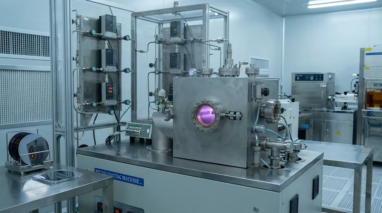
The entire process occurs inside a vacuum chamber where temperature, pressure, and gas flow are controlled with extreme precision. This control is what allows for the creation of uniform, pure, and defect-free films across the entire wafer.
Why CVD is Critical for Semiconductors
Building Insulating Layers (Dielectrics)
One of the most common uses of CVD is to deposit insulating films, such as silicon dioxide (SiO₂) or silicon nitride (Si₃N₄). These dielectric layers are essential for isolating different conductive components of a transistor from one another, preventing short circuits.
Creating Conductive Pathways (Metals)
CVD is also used to deposit conductive materials like tungsten or copper. These metal layers form the microscopic "wires" or interconnects that link the billions of transistors together to create a functioning integrated circuit.
Achieving Nanoscale Precision
Modern transistors have features that are only a few nanometers in size. CVD provides the atomic-level control necessary to build these structures repeatably and reliably across a massive scale, which is a requirement for manufacturing technologies like CMOS (Complementary Metal-Oxide-Semiconductor).
Understanding the Trade-offs and Challenges
Purity and Contamination
The performance of a semiconductor device is highly sensitive to impurities. The precursor gases used in CVD must be exceptionally pure, and the chamber must be impeccably clean to avoid introducing contaminating atoms that could ruin the chip.
Conformal Coverage
A major advantage of many CVD processes is their ability to create conformal films. This means the deposited layer uniformly coats all surfaces, including the vertical sidewalls of complex, microscopic trenches. This is incredibly difficult to achieve with other methods.
Temperature Sensitivity
Many CVD processes require high temperatures to drive the chemical reactions. These high temperatures can sometimes damage previously fabricated structures on the chip, forcing engineers to use alternative, lower-temperature deposition techniques for certain steps.
How to Apply This to Your Goal
- If your primary focus is electrical isolation: CVD is the industry-standard method for depositing high-quality silicon dioxide and silicon nitride dielectrics.
- If your primary focus is creating conductive interconnects: CVD is essential for depositing materials like tungsten to fill tiny vertical vias that connect different layers of circuitry.
- If your primary focus is building the transistor itself: CVD is used to deposit various semiconductor films, like polysilicon, which act as the gate that controls the flow of electricity.
Ultimately, Chemical Vapor Deposition is not just one process; it is a foundational technology that makes the precise construction of modern electronics possible.
Summary Table:
| CVD Application | Key Materials Deposited | Primary Function in Semiconductors |
|---|---|---|
| Insulating Layers | Silicon Dioxide (SiO₂), Silicon Nitride (Si₃N₄) | Electrically isolate transistor components |
| Conductive Pathways | Tungsten (W), Copper (Cu) | Form interconnects (wires) between transistors |
| Transistor Fabrication | Polysilicon | Create the transistor gate structure |
Ready to integrate precise CVD processes into your semiconductor R&D or production? KINTEK specializes in providing high-performance lab equipment and consumables for advanced material deposition. Our solutions help you achieve the nanoscale precision and purity required for next-generation microchips. Contact our experts today to discuss how we can support your laboratory's specific thin-film fabrication needs.
Visual Guide
Related Products
- Inclined Rotary Plasma Enhanced Chemical Vapor Deposition PECVD Equipment Tube Furnace Machine
- HFCVD Machine System Equipment for Drawing Die Nano-Diamond Coating
- 915MHz MPCVD Diamond Machine Microwave Plasma Chemical Vapor Deposition System Reactor
- Vacuum Hot Press Furnace Machine for Lamination and Heating
- 1200℃ Split Tube Furnace with Quartz Tube Laboratory Tubular Furnace
People Also Ask
- What are different types of thin films? A Guide to Function, Material, and Deposition Methods
- What is the difference between PECVD and APCVD? Choose the Right CVD Method for Your Application
- What is the process of PECVD in semiconductor? Enabling Low-Temperature Thin Film Deposition
- Can plasma enhanced CVD deposit metals? Why PECVD is rarely used for metal deposition
- How do PECVD systems improve DLC coatings on implants? Superior Durability and Biocompatibility Explained
