In Scanning Electron Microscopy (SEM), gold sputtering is a foundational sample preparation technique used to coat non-conductive or poorly-conductive specimens with an ultra-thin layer of gold. This process is essential because the electron beam used in an SEM requires a conductive surface to produce a clear, stable image. Without this coating, non-conductive samples build up a static charge, leading to severe image distortion and rendering the analysis useless.
The core problem with imaging materials like polymers, ceramics, or biological tissue in an SEM is that they don't conduct electricity. Gold sputtering solves this by creating a thin, conductive "shell" around the sample, allowing the electron beam to be grounded and enabling the capture of a high-quality, high-resolution image.

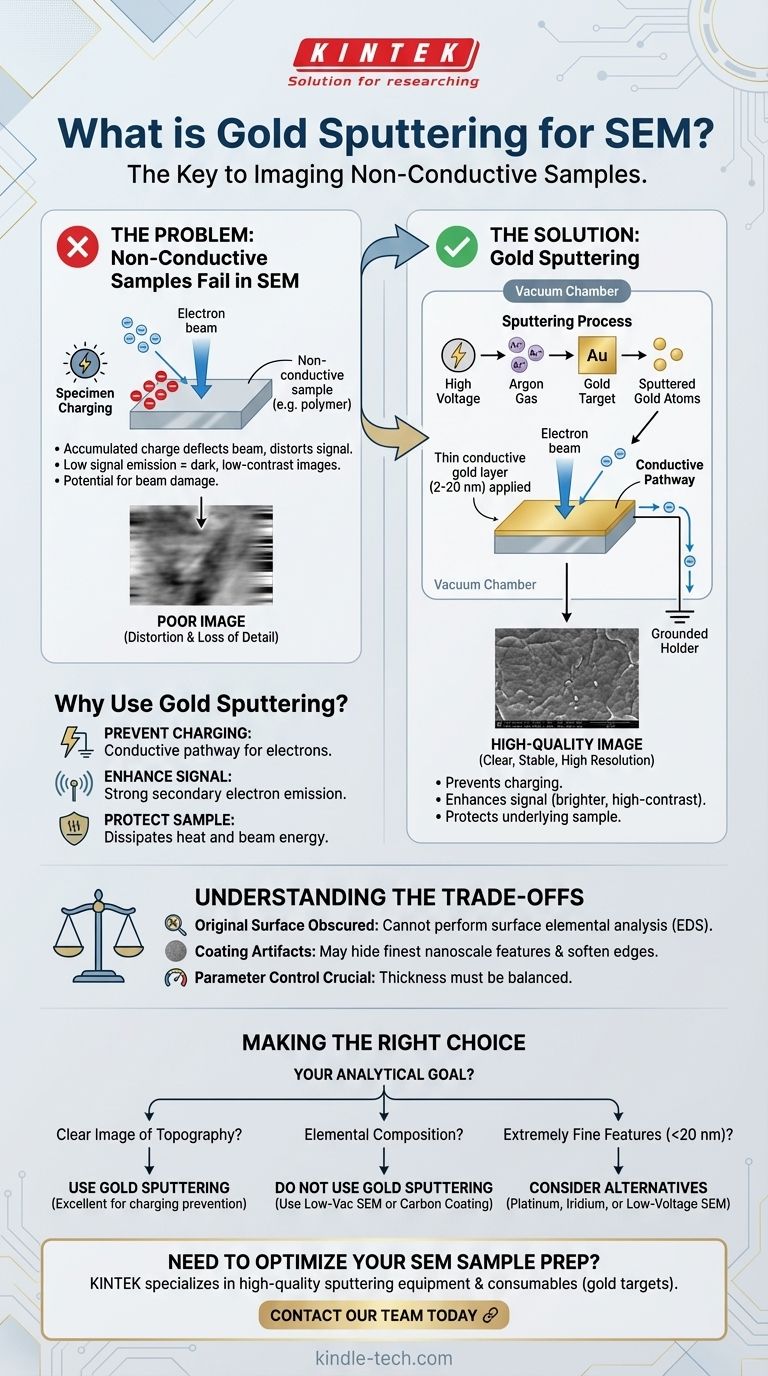
The Core Problem: Why Non-Conductive Samples Fail in SEM
To understand the purpose of gold sputtering, you must first understand the challenges inherent in imaging non-conductive materials with an electron beam.
The Issue of Specimen Charging
An SEM works by scanning a sample with a focused beam of electrons. When these electrons hit a conductive sample, they are safely conducted away to ground.
However, on a non-conductive surface, these electrons have nowhere to go. They accumulate in one area, creating a negative static charge that deflects the incoming electron beam and distorts the emitted signal, resulting in bright streaks, shifting, and a complete loss of image detail.
Low Signal Emission
The image in an SEM is primarily formed by detecting secondary electrons that are ejected from the sample's surface when hit by the main beam.
Many non-conductive materials are naturally poor emitters of these secondary electrons. This results in a weak signal, leading to dark, low-contrast images with a poor signal-to-noise ratio.
Potential for Beam Damage
The focused energy of the electron beam can damage delicate, beam-sensitive samples like polymers and biological tissues. This concentration of energy can cause the specimen to melt, burn, or deform.
How Gold Sputtering Solves the Problem
Sputter coating directly counteracts these issues by applying a thin metallic film, typically between 2 and 20 nanometers thick, onto the sample's surface.
The Sputtering Process Explained
In a vacuum chamber, a high voltage is used to ionize a gas (usually argon), creating a plasma. These ions are accelerated toward a target made of pure gold.
The impact of the ions ejects, or "sputters," individual gold atoms from the target. These gold atoms then travel and deposit onto the surface of the specimen, creating a uniform, thin film that conforms to its topography.
Creating a Conductive Pathway
This new gold layer provides an effective electrical pathway. As the electron beam scans the sample, the gold coating conducts the charge away to the grounded SEM specimen holder.
This single function completely prevents specimen charging, which is the most common cause of poor SEM images on non-conductive samples.
Enhancing the Image Signal
Gold is an excellent material for emitting secondary electrons. When the SEM's primary beam strikes the gold-coated surface, it generates a much stronger and more consistent signal than the original material would have.
This leads to a dramatic improvement in image brightness, contrast, and the overall signal-to-noise ratio.
Protecting the Underlying Sample
The conductive gold layer also acts as a protective barrier. It helps to dissipate the energy and heat from the electron beam across the surface, shielding the delicate underlying specimen from direct exposure and potential damage.
Understanding the Trade-offs of Gold Coating
While essential, gold sputtering is not without its compromises. It is a modification of the sample, and you must understand its limitations.
The Original Surface is Obscured
The most significant trade-off is that you are no longer imaging the sample's true surface; you are imaging the gold coating on top of it.
This means you cannot perform elemental analysis (like Energy Dispersive X-ray Spectroscopy, or EDS) on the surface, as the detector will primarily register the presence of gold.
Coating Artifacts Can Hide Features
The gold coating itself has a grain structure. While very fine, this structure can obscure the finest nanoscale details on the specimen's surface. The thickness of the coating can soften sharp edges and fill in tiny pores.
Parameter Control is Crucial
Achieving an optimal coating requires skill. The operator must correctly set parameters like coating time and current to control the film's thickness. A coating that is too thick will obscure details, while one that is too thin may not be effective at preventing charging.
Making the Right Choice for Your Analysis
Deciding whether to use gold sputtering depends entirely on your analytical goal.
- If your primary focus is obtaining a clear image of a non-conductive sample's topography: Gold sputtering is an excellent and often necessary choice to prevent charging and enhance the image signal.
- If your primary focus is determining the elemental composition of the surface: Do not use gold sputtering, as the coating will completely interfere with the analysis; consider using a low-vacuum SEM or carbon coating instead.
- If your primary focus is imaging extremely fine nanoscale features (under ~20 nm): Consider using a higher-performance, finer-grained coating material like platinum or iridium, or explore advanced low-voltage SEM techniques that may reduce the need for coating.
Ultimately, gold sputtering is a foundational tool that makes the vast world of non-conductive materials visible to the power of scanning electron microscopy.
Summary Table:
| Aspect | Impact of Gold Sputtering |
|---|---|
| Conductivity | Provides a pathway to ground, preventing charge buildup and image distortion. |
| Signal Quality | Enhances secondary electron emission for brighter, higher-contrast images. |
| Sample Protection | Dissipates beam energy, shielding delicate samples from damage. |
| Coating Thickness | Typically 2-20 nm; critical to balance conductivity with detail preservation. |
Need to optimize your SEM sample preparation? KINTEK specializes in providing high-quality sputtering equipment and consumables, including gold targets, to ensure your non-conductive samples are perfectly coated for clear, reliable SEM imaging. Our experts can help you select the right tools to prevent charging and enhance your analytical results. Contact our team today to discuss your specific laboratory needs!
Visual Guide
Related Products
- Inclined Rotary Plasma Enhanced Chemical Vapor Deposition PECVD Equipment Tube Furnace Machine
- RF PECVD System Radio Frequency Plasma-Enhanced Chemical Vapor Deposition RF PECVD
- Electron Beam Evaporation Coating Oxygen-Free Copper Crucible and Evaporation Boat
- Chemical Vapor Deposition CVD Equipment System Chamber Slide PECVD Tube Furnace with Liquid Gasifier PECVD Machine
- Microwave Plasma Chemical Vapor Deposition MPCVD Machine System Reactor for Lab and Diamond Growth
People Also Ask
- What is plasma in CVD process? Lowering Deposition Temperatures for Heat-Sensitive Materials
- What is plasma enhanced chemical vapor deposition? Achieve Low-Temperature, High-Quality Thin Films
- What is the difference between CVD and PECVD? Choose the Right Thin-Film Deposition Method
- How does plasma enhanced CVD work? Achieve Low-Temperature, High-Quality Thin Film Deposition
- What is meant by vapor deposition? A Guide to Atomic-Level Coating Technology