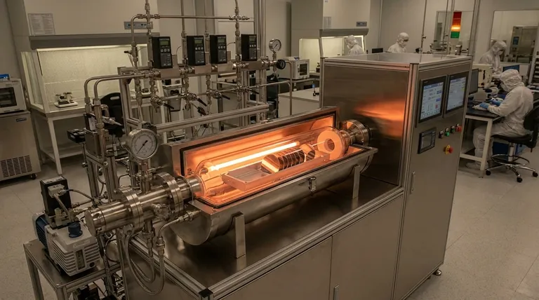
At its core, LPCVD stands for Low-Pressure Chemical Vapor Deposition. It is a foundational process in microfabrication and material science used to grow extremely high-quality, uniform thin films of material onto a substrate, such as a silicon wafer. This is achieved by reacting specific precursor gases on the substrate's surface within a high-temperature, low-pressure (vacuum) environment.
LPCVD is not just a manufacturing technique; it is the solution to a critical geometry problem in microelectronics. By reducing the chamber pressure, the process enables gas molecules to coat complex, three-dimensional microscopic structures with unparalleled uniformity, a property known as conformality.
How Chemical Vapor Deposition (CVD) Works
The Core Principle: From Gas to Solid
Chemical Vapor Deposition is a process where a solid material is formed on a heated surface from a chemical reaction in the gas phase.
Precursor gases, which contain the atoms you want to deposit (like silicon or nitrogen), are introduced into a reaction chamber. When these gases reach the hot substrate, they react or decompose, leaving behind the desired solid material as a thin film.
Key Components of the Process
The essential elements are a controlled chamber, a heat source to bring the substrate to the correct reaction temperature, and a system for precisely introducing the precursor gases. The quality of the final film depends on controlling temperature, pressure, and gas flow rates.
The "Low-Pressure" Advantage: Why It Matters
Operating the CVD process under low pressure (in a vacuum) is not a minor adjustment; it fundamentally changes the physics of the deposition and provides three critical benefits.
Unmatched Film Conformality
In a vacuum, there are far fewer gas molecules, which dramatically increases their mean free path—the average distance a molecule travels before colliding with another.
This allows the precursor gas molecules to diffuse deep into microscopic trenches and over sharp steps on the substrate surface before reacting. The result is a film that is almost perfectly uniform in thickness on all surfaces, which is known as high conformality. This is essential for building reliable, multi-layered integrated circuits.
Superior Purity and Batch Uniformity
The vacuum environment inherently removes atmospheric contaminants like oxygen, nitrogen, and water vapor, leading to a much purer deposited film.
Furthermore, the diffusion-dominant nature of gas transport at low pressure allows for excellent thickness uniformity across many wafers at once. This enables wafers to be stacked vertically in a "boat," significantly increasing manufacturing throughput compared to methods that require wafers to lie flat.
Driven by High Temperature
It is crucial to understand that standard LPCVD is a thermally driven process. The high temperatures, often ranging from 400°C to over 900°C, provide the energy needed to break the chemical bonds in the precursor gases and initiate the surface reaction.
Understanding the Trade-offs: LPCVD vs. Other Methods
No single deposition method is perfect for every application. Choosing the right one involves understanding its trade-offs against other common techniques.
LPCVD vs. PECVD (Plasma-Enhanced CVD)
The key difference here is temperature. PECVD uses an electric field to create plasma, which energizes the precursor gases. This allows deposition to occur at much lower temperatures (typically 200-400°C).
This makes PECVD essential for depositing films late in the manufacturing process, after temperature-sensitive components like aluminum interconnects have already been created. The trade-off is that PECVD films generally have lower quality, lower density, and poorer conformality than LPCVD films.
LPCVD vs. APCVD (Atmospheric Pressure CVD)
APCVD operates at normal atmospheric pressure. Its primary advantage is a very high deposition rate, making it useful for growing thick, simple layers where precision is less critical.
However, the short mean free path of gas molecules at atmospheric pressure results in very poor conformality, making it unsuitable for the complex topographies of modern microdevices.
LPCVD vs. PVD (Physical Vapor Deposition)
PVD techniques like sputtering are fundamentally different. They are physical, not chemical, processes that involve bombarding a solid target to eject atoms, which then coat a substrate.
PVD is a "line-of-sight" technique, meaning it has very poor conformality and struggles to coat sidewalls of trenches. It is primarily used for depositing metal films, whereas LPCVD excels at depositing dielectric and polysilicon layers.
Making the Right Choice for Your Goal
Selecting the correct deposition method requires matching the process capabilities to the material requirements and thermal budget of your device.
- If your primary focus is the highest film quality and conformality for a robust material: LPCVD is the definitive standard for layers like silicon nitride (Si₃N₄) and polysilicon.
- If your primary focus is depositing a passivation or dielectric layer at low temperatures: PECVD is the necessary choice to avoid damaging underlying structures.
- If your primary focus is the fastest deposition of a simple, thick film where conformality is not a concern: APCVD can be a cost-effective solution.
- If your primary focus is depositing a metal film for interconnects: A PVD method like sputtering is the industry-standard tool for the job.
Understanding the principles behind why each method works is the key to engineering truly advanced materials and devices.
Summary Table:
| Feature | LPCVD | PECVD | APCVD | PVD |
|---|---|---|---|---|
| Primary Driver | High Temperature | Plasma (Low Temp) | Atmospheric Pressure | Physical Sputtering |
| Typical Temperature | 400°C - 900°C+ | 200°C - 400°C | High | Variable |
| Film Conformality | Excellent (High) | Good | Poor | Poor (Line-of-sight) |
| Best For | High-quality dielectrics (e.g., Si₃N₄), Polysilicon | Low-temperature passivation layers | Thick, simple films | Metal films (interconnects) |
Need to deposit high-quality, uniform thin films for your research or production? KINTEK specializes in providing the precise lab equipment and consumables needed for advanced processes like LPCVD. Our expertise helps you achieve superior film conformality and purity for your microelectronics and material science applications. Contact our experts today to discuss your specific requirements and find the perfect solution for your laboratory needs.
Visual Guide

Related Products
- Chemical Vapor Deposition CVD Equipment System Chamber Slide PECVD Tube Furnace with Liquid Gasifier PECVD Machine
- Customer Made Versatile CVD Tube Furnace Chemical Vapor Deposition Chamber System Equipment
- Microwave Plasma Chemical Vapor Deposition MPCVD Machine System Reactor for Lab and Diamond Growth
- Inclined Rotary Plasma Enhanced Chemical Vapor Deposition PECVD Equipment Tube Furnace Machine
- 915MHz MPCVD Diamond Machine Microwave Plasma Chemical Vapor Deposition System Reactor
People Also Ask
- What are the processes of vapor phase deposition? Understand CVD vs. PVD for Superior Thin Films
- How expensive is chemical vapor deposition? Understanding the True Cost of High-Performance Coating
- What types of substrates are used in CVD to facilitate graphene films? Optimize Graphene Growth with the Right Catalyst
- Why is Chemical Vapor Deposition (CVD) equipment uniquely suited for constructing hierarchical superhydrophobic structures?
- What is the chemical vapor deposition growth process? Build Superior Thin Films from the Atom Up


