At its core, Physical Vapor Deposition (PVD) is a vacuum-based technique for applying an extremely thin layer of material onto a surface. Unlike chemical processes, PVD works by physically transforming a solid source material into a vapor, which then travels through the vacuum and condenses onto the target object, building the film atom by atom. This fundamental difference is what gives PVD coatings their high purity and exceptional performance characteristics.
The crucial distinction of PVD is its reliance on purely physical mechanisms—such as evaporation or ion bombardment—to transfer material in a vacuum. This avoids the chemical reactions inherent in other methods, resulting in coatings that are dense, pure, and highly durable.
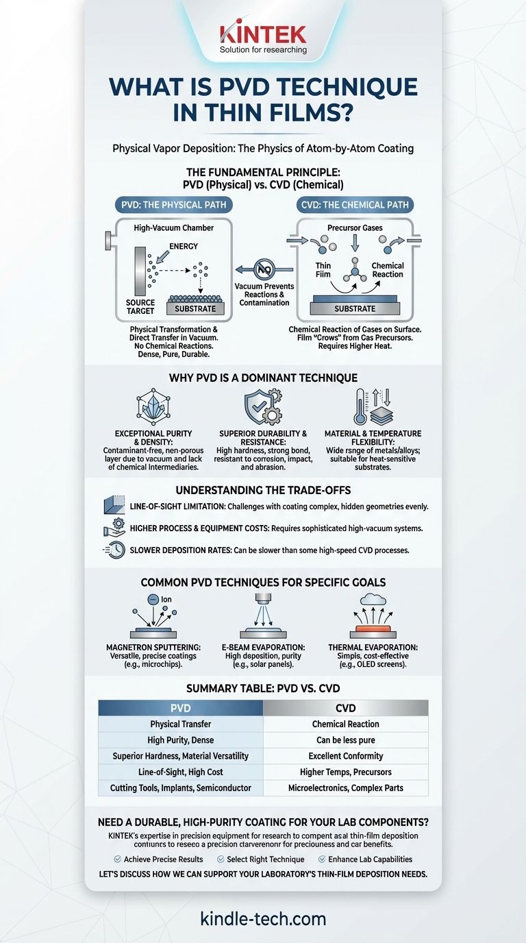
The Fundamental Principle: Physical vs. Chemical
To truly understand PVD, it's essential to contrast it with its main alternative, Chemical Vapor Deposition (CVD). Their names reveal their core difference.
How PVD Works (The Physical Path)
The PVD process involves three primary steps, all conducted within a high-vacuum chamber. First, a solid source material (the "target") is bombarded with energy, causing it to vaporize. Second, these vaporized atoms or molecules travel in a straight line through the vacuum. Finally, they land on and condense onto the substrate, forming a thin, uniform film.
The CVD Counterpart (The Chemical Path)
CVD, in contrast, does not physically transfer material. Instead, it introduces precursor gases into a chamber containing the substrate. A chemical reaction is then triggered on the substrate's surface, typically by high heat, causing a solid film to "grow" from the gases.
The Critical Role of the Vacuum
The vacuum environment is non-negotiable for PVD. It ensures that the vaporized atoms from the source can travel to the substrate without colliding with or reacting to other atoms, like those in the air. This guarantees the high purity and adhesion of the final coating.
Why PVD is a Dominant Technique
The physical nature of the PVD process gives its coatings several distinct advantages that make it the preferred choice for demanding applications in aerospace, semiconductors, medical devices, and cutting tools.
Exceptional Purity and Density
Because the material moves directly from a solid source to the substrate without intermediate chemical reactions, PVD films are exceptionally pure. The vacuum environment prevents contaminants from being incorporated into the coating, resulting in a dense, non-porous layer.
Superior Durability and Resistance
PVD coatings are renowned for their hardness and resilience. They create a strong bond with the substrate, making them highly resistant to corrosion, impact, and abrasion. This makes them ideal for protective layers on components that face high friction or harsh environments.
Material and Temperature Flexibility
The process can be used with a wide range of metals, alloys, and ceramics. Furthermore, because PVD can be performed at lower temperatures than many CVD processes, it is suitable for coating materials that cannot withstand high heat.
Understanding the Trade-offs
No single technology is a universal solution. While powerful, PVD has characteristics that make it unsuitable for certain scenarios.
Line-of-Sight Limitation
The "physical path" of PVD means atoms generally travel in straight lines. This makes it challenging to evenly coat complex, three-dimensional shapes with deep recesses or undercuts, as these areas are effectively in a shadow.
Process and Equipment Costs
PVD systems require high-vacuum chambers and sophisticated energy sources (like electron beams or magnetrons). This equipment represents a significant capital investment compared to simpler coating methods like electroplating.
Slower Deposition Rates
In some cases, PVD can have lower deposition rates compared to certain high-speed CVD processes. This can be a consideration for high-volume, low-cost manufacturing where cycle time is a critical factor.
Common PVD Techniques for Specific Goals
"PVD" is a family of techniques, each optimized for different materials and outcomes. The method chosen depends entirely on the application's requirements.
Magnetron Sputtering
In this technique, the source material is bombarded with energized ions, which "sputter" atoms off the target. It is highly versatile and widely used for creating precise electrical or optical coatings on products like microchips.
E-Beam Evaporation
An intense electron beam is focused on the source material, causing it to melt and evaporate. This method is valued for its high deposition rates and material purity, making it suitable for solar panels and architectural glass.
Thermal Evaporation
This is one of the simplest forms of PVD, where the source material is heated until it evaporates. It is a cost-effective method used for producing thin films for OLED screens and thin-film transistors.
Making the Right Choice for Your Application
Selecting the correct deposition technology requires aligning its capabilities with your primary objective.
- If your primary focus is maximum durability, purity, and performance: PVD is almost always the superior choice for creating hard, wear-resistant, and dense functional coatings.
- If your primary focus is coating complex, non-line-of-sight geometries: You should carefully evaluate if a gas-based process like CVD offers the necessary conformal coverage for your part.
- If your primary focus is high-volume coating of simple parts at the lowest cost: Other methods, such as electroplating or chemical bath deposition, may be more economically viable than PVD.
Ultimately, understanding PVD is about selecting a precision tool to construct materials with superior physical properties, one atomic layer at a time.
Summary Table:
| Key Aspect | PVD (Physical Vapor Deposition) | CVD (Chemical Vapor Deposition) |
|---|---|---|
| Core Process | Physical transfer of vaporized solid material | Chemical reaction of gases on the substrate surface |
| Coating Properties | High purity, dense, highly durable | Can be less pure, may have different structure |
| Advantages | Superior hardness, corrosion/abrasion resistance, works with many materials | Excellent conformity for complex 3D shapes |
| Limitations | Line-of-sight coating, higher equipment cost, slower deposition for some types | Often requires higher temperatures, involves chemical precursors |
| Common Applications | Cutting tools, medical implants, semiconductor layers, durable consumer goods | Microelectronics, complex component coatings |
Need a Durable, High-Purity Coating for Your Lab Components?
KINTEK specializes in precision lab equipment and consumables. Whether you're developing new materials, testing coatings, or require PVD-coated components for your research, we provide the reliable tools and expertise to ensure your success.
We help you:
- Achieve precise results with equipment designed for consistent, high-quality thin films.
- Select the right technique for your specific application, from sputtering to evaporation.
- Enhance your lab's capabilities with durable consumables and reliable systems.
Let's discuss how we can support your laboratory's thin-film deposition needs. Contact our experts today for a consultation!
Visual Guide
Related Products
- RF PECVD System Radio Frequency Plasma-Enhanced Chemical Vapor Deposition RF PECVD
- Split Chamber CVD Tube Furnace with Vacuum Station Chemical Vapor Deposition System Equipment Machine
- Chemical Vapor Deposition CVD Equipment System Chamber Slide PECVD Tube Furnace with Liquid Gasifier PECVD Machine
- VHP Sterilization Equipment Hydrogen Peroxide H2O2 Space Sterilizer
- Molybdenum Tungsten Tantalum Special Shape Evaporation Boat
People Also Ask
- What are the applications of PECVD? Essential for Semiconductors, MEMS, and Solar Cells
- What is plasma activated chemical vapour deposition method? A Low-Temperature Solution for Advanced Coatings
- How does RF power create plasma? Achieve Stable, High-Density Plasma for Your Applications
- Why is PECVD environment friendly? Understanding the Eco-Friendly Benefits of Plasma-Enhanced Coating
- What are the advantages of PECVD? Enable Low-Temperature, High-Quality Thin-Film Deposition


