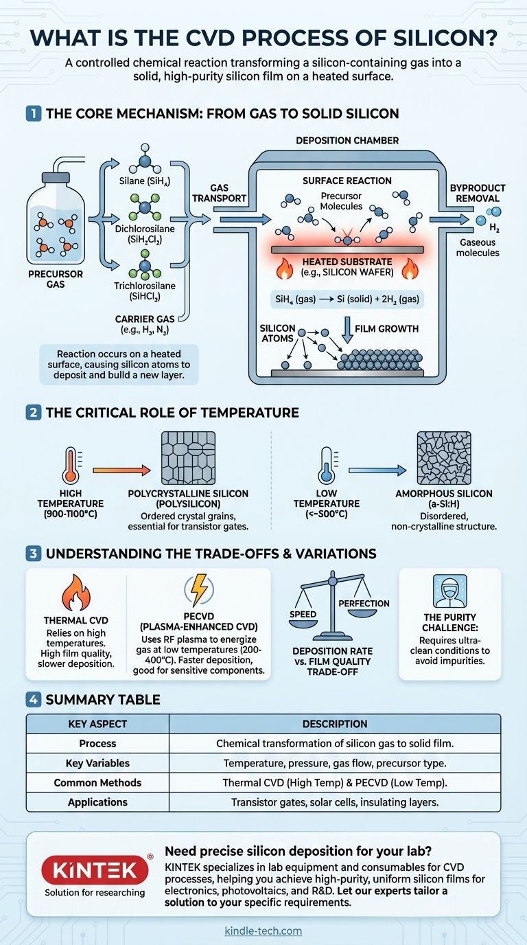
In essence, the Chemical Vapor Deposition (CVD) of silicon is a process that transforms a silicon-containing gas into a solid, high-purity silicon film on a heated surface. This is not a simple coating, but a controlled chemical reaction. Inside a specialized chamber, precursor gases are introduced and react on a hot substrate (like a silicon wafer), causing silicon atoms to break free and deposit onto the surface, building up a new layer atom by atom.
The core principle of silicon CVD is not merely 'coating' but a controlled chemical reaction. By precisely managing temperature, pressure, and gas flow, we can dictate how silicon atoms are released from a precursor gas and assemble themselves into a crystalline or amorphous solid film on a substrate.

The Core Mechanism: From Gas to Solid Silicon
To truly understand silicon CVD, you must view it as a precise, multi-step manufacturing process. Each step is critical for producing a film with the desired thickness, purity, and structure.
The Precursor Gas: The Source of Silicon
The process begins with a precursor gas, a volatile compound that contains silicon atoms. These gases are chosen because they decompose predictably at high temperatures.
Common precursors for silicon deposition include:
- Silane (SiH₄): Decomposes at relatively lower temperatures, but can be highly reactive.
- Dichlorosilane (SiH₂Cl₂): Offers a good balance of reactivity and safety.
- Trichlorosilane (SiHCl₃): Primarily used for producing high-purity bulk polysilicon for the electronics industry.
These precursors are often diluted with a carrier gas, such as hydrogen (H₂) or nitrogen (N₂), to control the reaction rate and ensure uniform delivery.
The Deposition Process: A Step-by-Step Reaction
The transformation from gas to solid film unfolds in a sequence of physical and chemical events within the reaction chamber.
- Gas Transport: The precursor and carrier gases are injected into the chamber and flow towards the heated substrate.
- Surface Reaction: When precursor molecules strike the hot substrate surface, they gain enough thermal energy to break their chemical bonds. For example, silane decomposes into solid silicon and hydrogen gas:
SiH₄ (gas) → Si (solid) + 2H₂ (gas). - Film Growth: The newly freed silicon atoms are highly reactive and bond to the substrate's surface. They migrate across the surface until they find a stable site, building upon the crystal lattice and forming a continuous film.
- Byproduct Removal: The gaseous byproducts of the reaction (like H₂ in the example above) are continuously pumped out of the chamber. This prevents them from interfering with the reaction and maintains the purity of the growing film.
The Critical Role of Temperature
Temperature is the most critical control knob in the CVD process. It directly dictates the rate of reaction and, more importantly, the final structure of the silicon film.
- Polycrystalline Silicon (Polysilicon): At high temperatures (typically 900-1100°C), deposited atoms have enough energy to move around and align themselves into small, ordered crystal grains. This "polysilicon" is essential for applications like transistor gates.
- Amorphous Silicon (a-Si:H): At lower temperatures (below ~500°C), atoms have less energy and essentially "stick" where they land, creating a disordered, non-crystalline structure.
Understanding the Trade-offs and Variations
The basic thermal CVD process is not the only option. The choice of method involves balancing competing priorities like processing temperature, deposition speed, and film quality.
Thermal CVD vs. Plasma-Enhanced CVD (PECVD)
The process described thus far is Thermal CVD, which relies solely on high temperatures to initiate the reaction.
Plasma-Enhanced CVD (PECVD) is a critical variation. It uses an RF plasma to energize the precursor gas, breaking it down into reactive ions and radicals. This allows deposition to occur at much lower temperatures (e.g., 200-400°C), which is vital for depositing films on devices that already have metal layers or other temperature-sensitive components.
Deposition Rate vs. Film Quality
There is a fundamental trade-off between speed and perfection. Increasing the temperature and precursor concentration can accelerate the deposition rate, but it can also lead to a less uniform film with more structural defects. High-quality electronic applications often require slower, more controlled deposition to achieve a near-perfect atomic structure.
The Purity Challenge
CVD is highly sensitive to contamination. Any unwanted molecules in the gas stream or the chamber can become incorporated into the growing silicon film as impurities. These impurities can drastically alter the film's electrical properties, making process purity and cleanroom conditions paramount.
How to Apply This to Your Goal
The specific CVD process you choose is dictated entirely by the final application of the silicon film.
- If your primary focus is creating gate electrodes in a transistor: You will use a thermal CVD process, likely with silane, to deposit a high-quality, conductive polycrystalline silicon film at high temperatures.
- If your primary focus is depositing a final insulating layer on a finished chip: You must use a low-temperature PECVD process to avoid melting the aluminum interconnects or damaging other components already fabricated on the wafer.
- If your primary focus is manufacturing bulk silicon for solar cells: You will use a high-rate, high-temperature process like the Siemens method, which uses trichlorosilane to produce large quantities of high-purity polysilicon.
Ultimately, mastering silicon CVD is about precisely controlling a chemical reaction to build a solid material, atom by atom, for a specific electronic purpose.
Summary Table:
| Key Aspect | Description |
|---|---|
| Process | Chemical transformation of silicon-containing gas into a solid film on a heated substrate. |
| Key Variables | Temperature, pressure, gas flow, and precursor type (e.g., Silane, Dichlorosilane). |
| Common Methods | Thermal CVD (high temp) and Plasma-Enhanced CVD (PECVD, low temp). |
| Applications | Transistor gates, solar cells, insulating layers on chips. |
Need precise silicon deposition for your lab? KINTEK specializes in lab equipment and consumables for CVD processes, helping you achieve high-purity, uniform silicon films for electronics, photovoltaics, and R&D. Let our experts tailor a solution to your specific temperature, purity, and throughput requirements. Contact us today to discuss your project!
Visual Guide
Related Products
- HFCVD Machine System Equipment for Drawing Die Nano-Diamond Coating
- Chemical Vapor Deposition CVD Equipment System Chamber Slide PECVD Tube Furnace with Liquid Gasifier PECVD Machine
- Customer Made Versatile CVD Tube Furnace Chemical Vapor Deposition Chamber System Equipment
- Cylindrical Resonator MPCVD Machine System Reactor for Microwave Plasma Chemical Vapor Deposition and Lab Diamond Growth
- 915MHz MPCVD Diamond Machine Microwave Plasma Chemical Vapor Deposition System Reactor
People Also Ask
- Why is Chemical Vapor Deposition (CVD) equipment uniquely suited for constructing hierarchical superhydrophobic structures?
- What are the advantages of chemical vapor deposition? Achieve Superior Thin Films for Your Lab
- What are the disadvantages and challenges of the HFCVD method? Overcome Growth Limits and Filament Issues
- What is the full form of HFCVD? A Guide to Hot Filament Chemical Vapor Deposition
- What is the hot filament chemical vapour deposition of diamond? A Guide to Synthetic Diamond Coating


