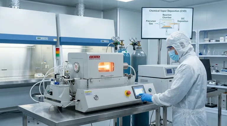
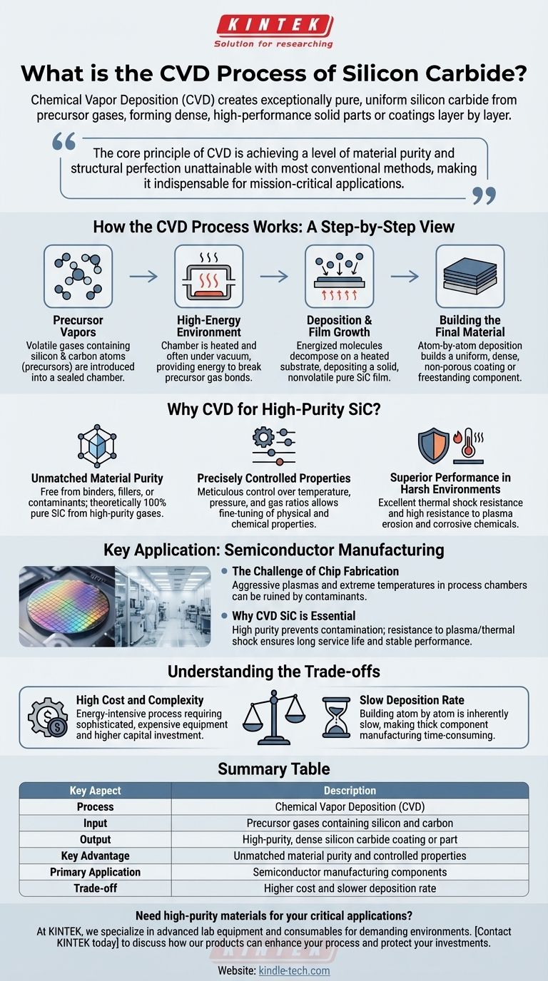
In essence, the Chemical Vapor Deposition (CVD) process for silicon carbide is a highly controlled manufacturing method used to grow an exceptionally pure and uniform solid material from a gas. Volatile precursor gases containing silicon and carbon are introduced into a high-temperature reaction chamber, where they decompose on a heated surface (the substrate) to form a dense, high-performance silicon carbide coating or solid part, layer by layer.
The core principle of CVD is not just about creating silicon carbide, but about achieving a level of material purity and structural perfection that is unattainable with most conventional methods. This precision is what makes it indispensable for mission-critical, high-technology applications.
How the CVD Process Works: A Step-by-Step View
The CVD process transforms simple gases into a highly advanced solid material through a carefully orchestrated series of physical and chemical events.
The Precursor Vapors
The process begins by introducing specific volatile gases, known as precursors, into a sealed reaction chamber. These gases are selected because they contain the necessary silicon and carbon atoms and will react predictably at high temperatures.
The High-Energy Environment
The chamber is heated to a precise reaction temperature, often while under a vacuum. This combination of heat and low pressure provides the necessary energy to break the chemical bonds within the precursor gas molecules.
Deposition and Film Growth
Inside the chamber, a substrate material is heated. When the energized gas molecules come into contact with this hot surface, they undergo a chemical reaction or decomposition. This reaction deposits a solid, nonvolatile film of pure silicon carbide (SiC) directly onto the substrate.
Building the Final Material
This deposition occurs atom by atom, building up a thin film that is perfectly uniform and covers all exposed areas of the substrate. Over time, these layers accumulate to create a coating or even a freestanding solid component with a dense, non-porous structure.
Why CVD is the Method of Choice for High-Purity SiC
While other methods can produce silicon carbide, CVD is chosen when performance and purity are the most critical factors. Its advantages stem directly from the nature of the process.
Unmatched Material Purity
Because the material is built directly from filtered, high-purity gases, the final silicon carbide product is free from the binders, fillers, or contaminants often present in traditional ceramic processes. This results in a material that is theoretically 100% pure SiC.
Precisely Controlled Properties
Engineers have meticulous control over the final material. By adjusting parameters like temperature, pressure, and the ratio of precursor gases, they can fine-tune the physical and chemical properties of the silicon carbide to meet exact specifications.
Superior Performance in Harsh Environments
The resulting material exhibits exceptional characteristics. It has excellent thermal shock resistance, meaning it can withstand rapid temperature changes without cracking. It is also highly resistant to erosion from the high-energy plasmas and corrosive chemicals used in advanced manufacturing.
Key Application: Semiconductor Manufacturing
The unique properties of CVD silicon carbide make it a critical material in the semiconductor industry, where environments are extremely demanding.
The Challenge of Chip Fabrication
Semiconductor process chambers, particularly those for oxide etching and rapid thermal processing (RTP), involve aggressive plasmas and extreme temperature cycles. Any contamination from equipment components can ruin an entire wafer of microchips, costing millions.
Why CVD SiC is Essential
CVD SiC is the ideal material for components inside these chambers. Its high purity ensures it does not introduce contaminants into the process. Its resistance to plasma erosion and thermal shock guarantees a long service life and stable performance, protecting the delicate silicon wafers.
Understanding the Trade-offs
Despite its clear advantages, the CVD process is not a universal solution. A trusted advisor must acknowledge its inherent trade-offs.
High Cost and Complexity
CVD is a complex, energy-intensive process requiring sophisticated and expensive equipment. The capital investment and operational costs are significantly higher than for methods like sintering or reaction bonding.
Slow Deposition Rate
Building a material atom by atom is inherently slow. Manufacturing thick, bulk components via CVD can take a very long time, which further contributes to the cost and limits its use for applications where speed and volume are the primary drivers.
Making the Right Choice for Your Application
Selecting the correct material and process requires a clear understanding of your project's primary goal.
- If your primary focus is extreme purity and performance: Specify CVD SiC for applications where material failure or contamination is not an option, such as in semiconductor process equipment.
- If your primary focus is resistance to harsh environments: Choose CVD SiC for components that will be exposed to aggressive chemicals, high-energy plasmas, or rapid and extreme temperature changes.
- If your primary focus is cost-sensitivity on a bulk component: You must evaluate if the superior properties of CVD justify its higher cost compared to other manufacturing methods for silicon carbide.
Ultimately, understanding the CVD process is key to leveraging silicon carbide's full potential in the world's most demanding technological applications.
Summary Table:
| Key Aspect | Description |
|---|---|
| Process | Chemical Vapor Deposition (CVD) |
| Input | Precursor gases containing silicon and carbon |
| Output | High-purity, dense silicon carbide coating or part |
| Key Advantage | Unmatched material purity and controlled properties |
| Primary Application | Semiconductor manufacturing components |
| Trade-off | Higher cost and slower deposition rate |
Need high-purity materials for your critical applications?
The CVD process is essential for creating silicon carbide that performs reliably in the most demanding environments, like semiconductor fabrication. At KINTEK, we specialize in providing advanced lab equipment and consumables that meet these stringent requirements.
Let us help you achieve superior results. Our expertise ensures you get the right solutions for your laboratory's specific challenges in material science and high-tech manufacturing.
Contact KINTEK today to discuss how our products can enhance your process and protect your investments.
Visual Guide
Related Products
- Silicon Carbide (SIC) Ceramic Sheet Wear-Resistant Engineering Advanced Fine Ceramics
- Silicon Carbide (SIC) Ceramic Plate for Engineering Advanced Fine Ceramics
- Silicon Carbide (SIC) Ceramic Sheet Flat Corrugated Heat Sink for Engineering Advanced Fine Ceramics
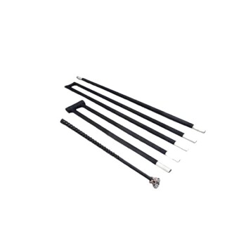
- Silicon Carbide SiC Thermal Heating Elements for Electric Furnace
- CVD Diamond for Thermal Management Applications
People Also Ask
- What are the uses of silicon carbide ceramics in different industries? Master Extreme Performance in Aerospace, Semiconductors & More
- What are the applications of silicon carbide? From Abrasives to High-Tech Semiconductors
- What is the temperature resistance of silicon carbide? Withstands Extreme Heat Up to 1500°C
- What are the properties of SiC? Unlock High-Temperature, High-Frequency Performance
- What are the common uses of silicon carbide? Unlock Extreme Performance in Harsh Environments