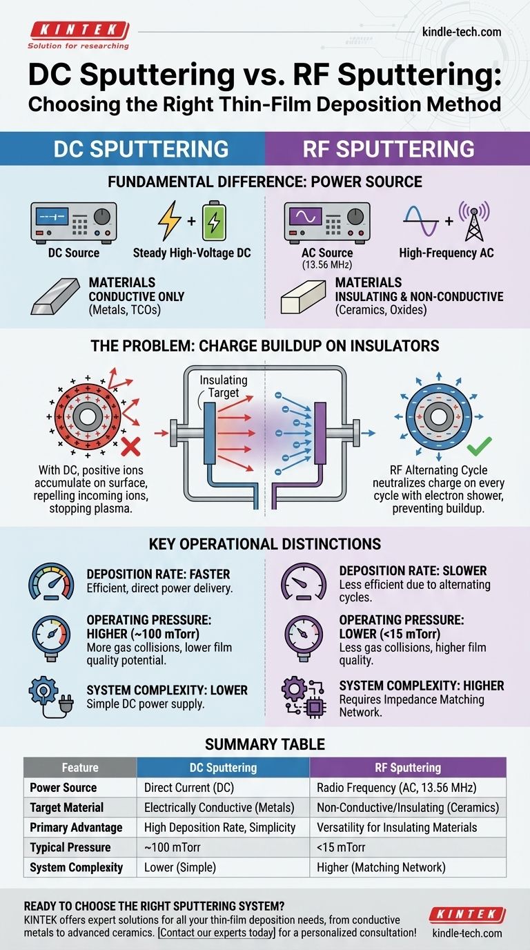
The fundamental difference between DC and RF sputtering lies in the type of electrical power source used to generate the plasma. DC (Direct Current) sputtering uses a steady, high-voltage DC source, making it suitable for conductive materials. RF (Radio Frequency) sputtering uses a high-frequency AC source, which allows it to deposit insulating, non-conductive materials by preventing a fatal buildup of electrical charge on the target.
The core decision between DC and RF sputtering is dictated entirely by the electrical properties of your target material. DC is a simple, high-rate process for conductors, while RF is the necessary solution for depositing insulators.
The Problem of Charge Buildup
The choice between DC and RF is not arbitrary; it solves a fundamental physics problem that occurs during the sputtering process. Understanding this problem is key to understanding the technologies.
How DC Sputtering Works
In a standard DC sputtering system, the material you want to deposit (the target) is given a strong negative DC voltage, making it the cathode.
The chamber is filled with an inert gas like argon. The high voltage ignites a plasma, creating positively charged argon ions. These positive ions are aggressively accelerated toward the negatively charged target, striking it with enough force to knock atoms loose, which then deposit onto your substrate.
The Insulator Failure Point
This process works perfectly as long as the target material is electrically conductive. A conductive target can easily dissipate the positive charge delivered by the constantly arriving argon ions.
If you try this with an insulating target (like a ceramic), positive charge accumulates rapidly on its surface. This buildup, often called "target poisoning," eventually repels the incoming positive argon ions, extinguishing the plasma and stopping the sputtering process entirely.
The RF Sputtering Solution
RF sputtering solves this by using an AC power source that alternates its polarity at a radio frequency, typically 13.56 MHz.
This rapid switching means the target is only negative for a very short period. During this negative half-cycle, ion bombardment and sputtering occur just like in a DC system.
Crucially, during the subsequent positive half-cycle, the target attracts a shower of electrons from the plasma. These electrons instantly neutralize the positive charge that built up during the sputtering phase. This "self-cleaning" action on every cycle prevents charge accumulation, allowing for the continuous sputtering of insulating materials.
Key Operational Distinctions
The difference in power source creates several other important operational distinctions between the two methods.
Material Capability
This is the defining factor. DC sputtering is primarily for conductive materials, like most metals and transparent conductive oxides. RF sputtering is for non-conductive materials, such as ceramics, oxides, and other dielectrics.
Plasma and Operating Pressure
RF fields are more efficient at energizing electrons to sustain a plasma. Because of this, RF sputtering can operate at much lower gas pressures (often below 15 mTorr) compared to DC sputtering (closer to 100 mTorr).
Lower pressure reduces the chance that sputtered atoms will collide with gas molecules on their way to the substrate. This results in a more direct, line-of-sight deposition, which can lead to higher-quality films.
Deposition Rates
For materials that can be deposited by either method (conductors), DC sputtering generally offers a higher deposition rate. Its power delivery is more direct and efficient.
RF sputtering is inherently less efficient due to the alternating cycles and the complexity of its power delivery system, resulting in slower deposition.
System Complexity
A DC sputtering power supply is a relatively simple high-voltage DC source. An RF system is more complex, requiring an impedance matching network between the power supply and the chamber to ensure efficient power transfer to the plasma.
Understanding the Trade-offs
Choosing a method involves balancing the capabilities of each technology against your specific goals.
The Advantage of DC: Speed and Simplicity
For conductive films, DC sputtering is the clear winner. It is a faster, more efficient, and less complex process that delivers high-quality metallic layers. Its only major limitation is its inability to handle insulators.
The Advantage of RF: Material Versatility
The primary benefit of RF sputtering is its ability to deposit virtually any material, regardless of its electrical conductivity. This versatility makes it essential for producing advanced optical coatings, dielectric layers, and complex ceramic films.
The Consequence: Complexity and Rate
This versatility comes at the cost of slower deposition rates and a more complex and expensive system. The RF power supply and its required impedance matching network represent a significant increase in system complexity compared to a simple DC setup.
Making the Right Choice for Your Material
Your decision should be based directly on the electrical characteristics of the material you intend to deposit.
- If your primary focus is depositing conductive films (like most metals): DC sputtering is the more efficient, faster, and simpler choice.
- If your primary focus is depositing insulating or dielectric films (like ceramics or oxides): RF sputtering is the necessary and correct technology to use.
Ultimately, selecting the right sputtering technique is about matching the tool to the fundamental properties of your material.
Summary Table:
| Feature | DC Sputtering | RF Sputtering |
|---|---|---|
| Power Source | Direct Current (DC) | Radio Frequency (AC, 13.56 MHz) |
| Target Material | Electrically Conductive (Metals) | Non-Conductive/Insulating (Ceramics, Oxides) |
| Primary Advantage | High Deposition Rate, Simplicity | Versatility for Insulating Materials |
| Typical Operating Pressure | ~100 mTorr | < 15 mTorr |
| System Complexity | Lower (Simple DC Power Supply) | Higher (Requires Impedance Matching Network) |
Ready to choose the right sputtering system for your lab's unique needs?
Whether you're working with conductive metals or advanced insulating ceramics, KINTEK has the expertise and equipment to support your thin-film deposition projects. Our range of DC and RF sputtering systems is designed to deliver precision, reliability, and high-quality results.
Let KINTEK, your trusted lab equipment partner, help you optimize your process. Contact our experts today for a personalized consultation!
Visual Guide