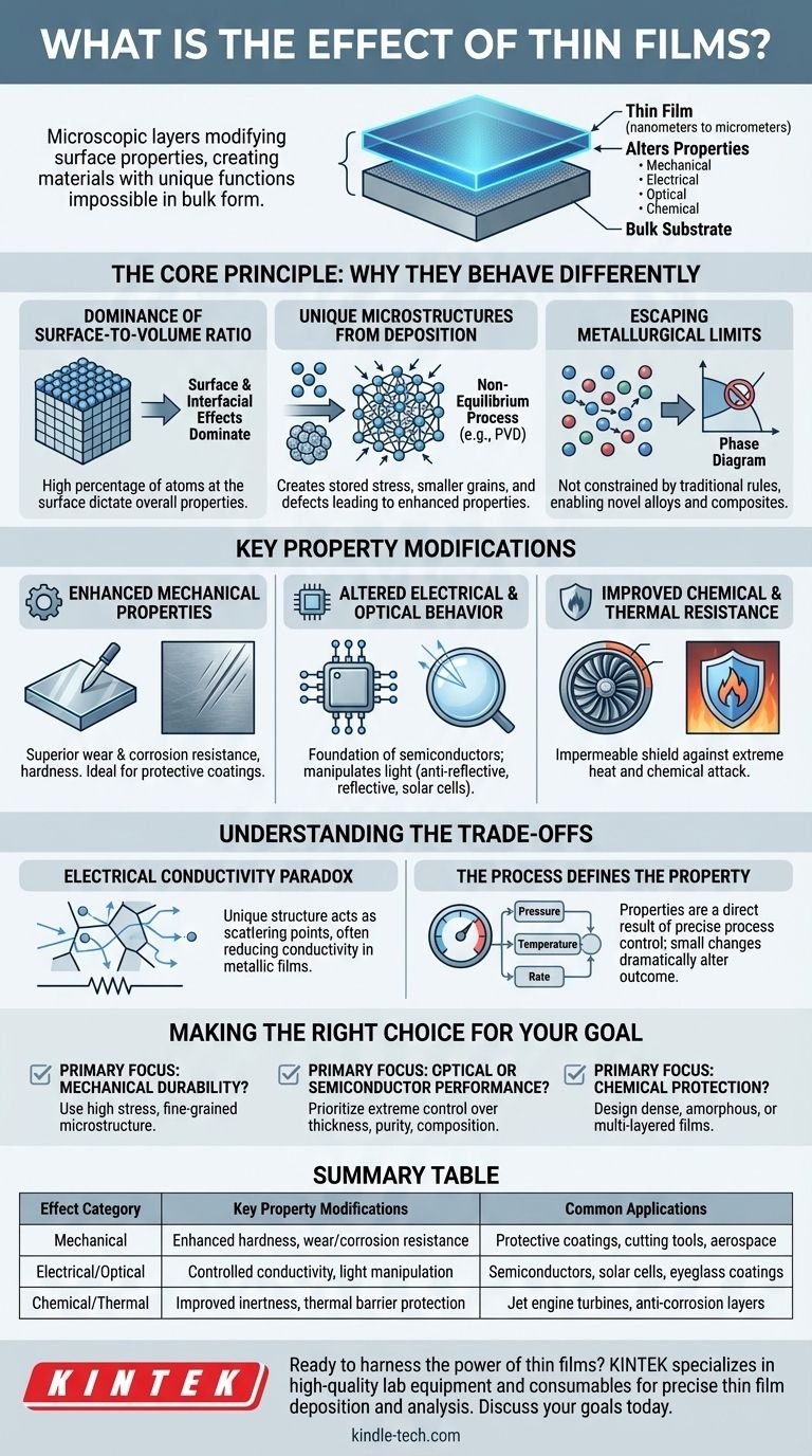
At their core, thin films are microscopic layers of material, ranging from a few nanometers to several micrometers thick, that are deposited onto a surface to fundamentally alter its properties. Their primary effect is to give a bulk material new mechanical, electrical, optical, or chemical characteristics without changing the underlying substrate itself. This allows for the creation of high-performance components with unique and tailored functions.
The defining effect of a thin film is the creation of a material with properties that are impossible to achieve in its bulk form. This is because at such a small scale, the physics of surfaces and interfaces dominates the conventional physics of the material's volume.
The Core Principle: Why Thin Films Behave Differently
To understand the effects of thin films, you must first understand why they are fundamentally different from bulk materials. The unique behavior arises from manipulating matter at a scale where new rules apply.
The Dominance of Surface-to-Volume Ratio
In any bulk material, the vast majority of atoms are surrounded by other atoms. In a thin film, a significant percentage of atoms are either at the surface or at the interface with the substrate.
This high surface-to-volume ratio means that surface energy and interfacial effects, which are negligible in bulk materials, become dominant forces that dictate the film's overall properties.
Unique Microstructures from Deposition
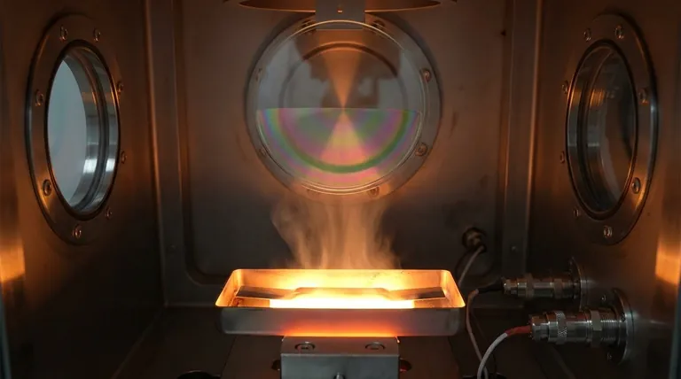
Most thin films are created using non-equilibrium deposition processes like physical vapor deposition (PVD). This method "freezes" atoms into a high-energy state.
This creates a unique microstructure filled with stored stress, smaller grain sizes, and a higher density of features like grain boundaries and dislocations. These are often considered "defects" in bulk materials, but in thin films, they are precisely what lead to enhanced properties like greater hardness and strength.
Escaping Metallurgical Limits
Traditional material creation is bound by the rules of metallurgy and phase diagrams, which dictate which elements can be mixed and in what proportions.
Because thin film deposition is a non-equilibrium process, it is not constrained by these phase diagrams. This allows engineers to create novel alloys and composite structures that simply could not exist in a bulk form, opening up entirely new possibilities for material science.
Key Property Modifications
The principles of thin films translate into a wide range of practical effects. These modifications are the reason thin films are ubiquitous in modern technology.
Enhanced Mechanical Properties
By controlling the microstructure, thin films can be made exceptionally hard and durable. The fine grain structure and internal stresses act as barriers that prevent the material from deforming.
This results in superior wear resistance, corrosion resistance, and overall durability, making them ideal as protective coatings on everything from machine tools to aerospace components.
Altered Electrical and Optical Behavior
Thin films are the foundation of the semiconductor industry. By layering different materials with nanometer precision, we can control the flow of electrons to create transistors and memory devices.
They also manipulate light. Anti-reflective coatings on eyeglasses, reflective layers in mirrors, and light-absorbing layers in solar cells are all applications that depend on a film's thickness and refractive index.
Improved Chemical and Thermal Resistance
A dense, non-porous thin film can act as an impermeable shield between a material and its environment.
This is the principle behind thermal barrier coatings on jet engine turbines, which protect the underlying metal from extreme heat, and anti-corrosion coatings that prevent chemical attack.
Understanding the Trade-offs
While powerful, the effects of thin films are not without their complexities and potential downsides. An objective understanding requires acknowledging these trade-offs.
The Electrical Conductivity Paradox
While essential for semiconductors, the unique structure of a thin film often reduces electrical conductivity in metallic films compared to their bulk counterparts.
The same grain boundaries and defects that increase hardness also act as scattering points for electrons. This shortens the "mean free path" of charge carriers, increasing electrical resistance. This is a critical consideration for applications requiring high conductivity.
The Process Defines the Property
The properties of a thin film are not inherent; they are a direct result of the deposition process. Small changes in pressure, temperature, or deposition rate can dramatically alter the film's stress, density, and microstructure.
This means that achieving a specific, repeatable effect requires extremely precise process control. A beneficial compressive stress in one scenario could become a detrimental stress that causes film delamination in another.
Substrate Adhesion is Critical
A thin film is only as effective as its bond to the substrate. Poor adhesion is a primary failure mode.
Factors like substrate cleanliness, surface roughness, and the choice of an intermediate "adhesion layer" are just as important as the properties of the film itself. Without a strong bond, even the most advanced film is useless.
Making the Right Choice for Your Goal
The "best" thin film effect is entirely dependent on your application. Your design choice should be guided by your primary objective.
- If your primary focus is mechanical durability: Use deposition methods that create high internal compressive stress and a dense, fine-grained microstructure for maximum hardness and wear resistance.
- If your primary focus is optical or semiconductor performance: Prioritize extreme control over film thickness, purity, and composition to precisely manipulate light or charge carriers.
- If your primary focus is chemical protection: Design a dense, amorphous, or multi-layered film that eliminates pathways for corrosive agents or heat to reach the substrate.
Ultimately, leveraging the effects of thin films is an exercise in controlling matter at the atomic scale to achieve a specific outcome.
Summary Table:
| Effect Category | Key Property Modifications | Common Applications |
|---|---|---|
| Mechanical | Enhanced hardness, wear resistance, corrosion resistance | Protective coatings, cutting tools, aerospace components |
| Electrical/Optical | Controlled conductivity, light manipulation (anti-reflective, reflective) | Semiconductors, solar cells, eyeglass coatings |
| Chemical/Thermal | Improved chemical inertness, thermal barrier protection | Jet engine turbines, anti-corrosion layers |
Ready to harness the power of thin films for your laboratory or production needs?
At KINTEK, we specialize in providing high-quality lab equipment and consumables for precise thin film deposition and analysis. Whether you're developing protective coatings, semiconductor devices, or advanced optical components, our solutions ensure the accuracy and repeatability your research demands.
Contact us today to discuss how our expertise can help you achieve your material science goals. Get in touch now!
Visual Guide
Related Products
- Aluminized Ceramic Evaporation Boat for Thin Film Deposition
- Tungsten Evaporation Boat for Thin Film Deposition
- Electron Beam Evaporation Coating Oxygen-Free Copper Crucible and Evaporation Boat
- Molybdenum Tungsten Tantalum Evaporation Boat for High Temperature Applications
- Aluminum-Plastic Flexible Packaging Film for Lithium Battery Packaging
People Also Ask
- What is thin film deposition? Unlock Advanced Surface Engineering for Your Materials
- What are the applications of thin films deposition? Unlock New Possibilities for Your Materials
- Why is an alumina boat and Ti3AlC2 powder bed necessary for Ti2AlC sintering? Protect MAX Phase Purity
- What is the widely used boat made of in thermal evaporation? Choosing the Right Material for High-Purity Deposition
- What are the alternatives to sputtering? Choose the Right Thin Film Deposition Method


