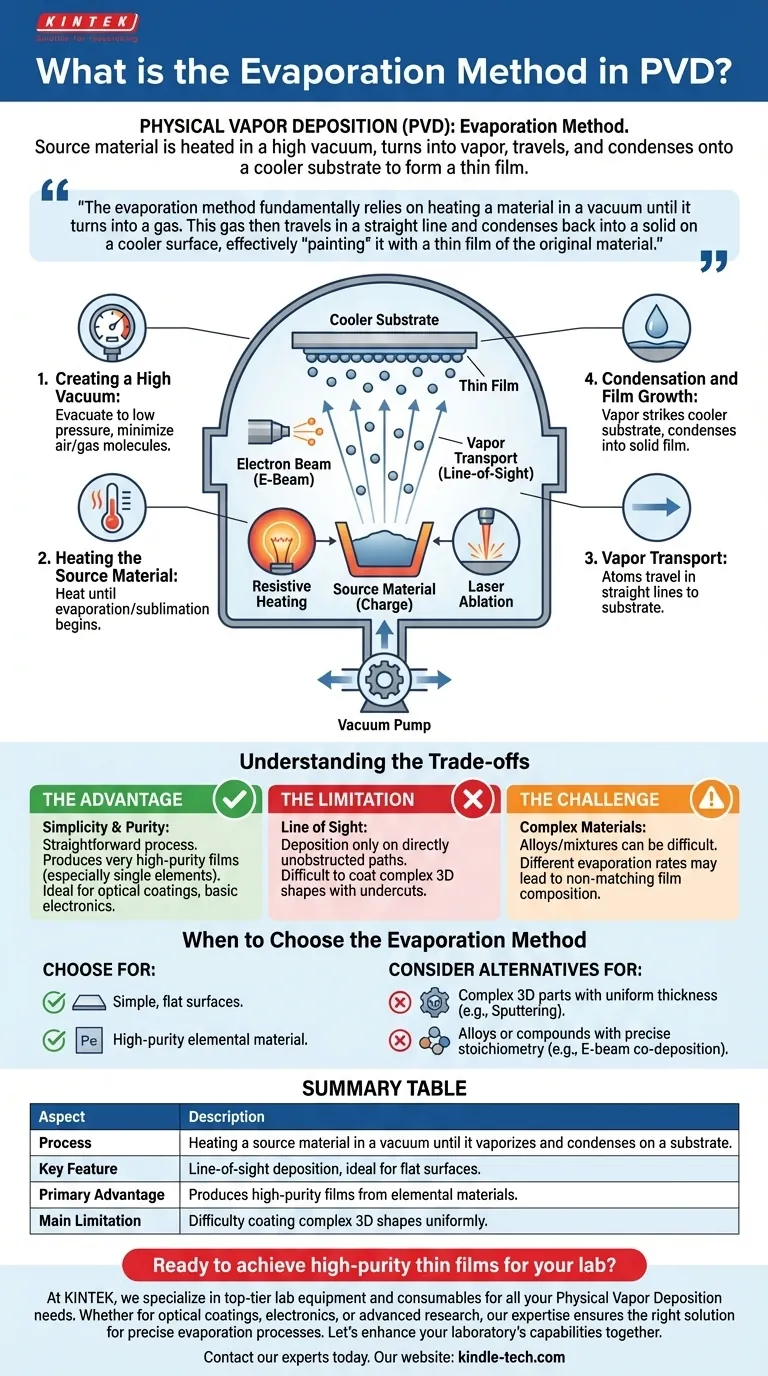
In Physical Vapor Deposition (PVD), the evaporation method is a process where a source material is heated in a high vacuum chamber until it melts and turns into a vapor. These vaporized atoms travel through the vacuum and then condense onto a cooler target object, known as the substrate. This condensation builds up, layer by layer, to form a thin, solid film on the substrate's surface.
The evaporation method fundamentally relies on heating a material in a vacuum until it turns into a gas. This gas then travels in a straight line and condenses back into a solid on a cooler surface, effectively "painting" it with a thin film of the original material.
How Evaporation PVD Works: The Core Process
The entire process happens within a high vacuum chamber, a critical condition for success. Each step is designed to ensure a pure, well-adhered film.
Step 1: Creating a High Vacuum
Before heating begins, the chamber is evacuated to a very low pressure. This high vacuum is essential to minimize the presence of air and other gas molecules that could collide with the vapor atoms, cause unwanted chemical reactions, or become trapped in the final coating.
Step 2: Heating the Source Material
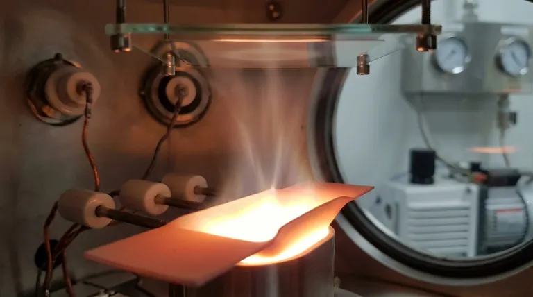
The source material, or "charge," is heated until it reaches a temperature where it begins to rapidly evaporate (turn to gas) or sublimate (go directly from solid to gas).
This heating can be accomplished through several techniques, including:
- Resistive Heating: Passing a high electrical current through a filament or "boat" holding the material.
- Electron Beam (E-Beam): Firing a focused beam of high-energy electrons at the source material.
- Laser Ablation: Using a high-power laser to vaporize the material's surface.
Step 3: Vapor Transport
Once vaporized, the material's atoms travel away from the source in a straight-line trajectory. This is often referred to as line-of-sight transport. Because of the high vacuum, there is nothing to impede their path from the source to the substrate.
Step 4: Condensation and Film Growth
When the hot vapor atoms strike the cooler substrate, they rapidly lose energy and condense back into a solid state. This process builds a thin film on the substrate's surface. The temperature of the substrate itself is often controlled to improve the film's adhesion and ensure a uniform structure.
Understanding the Trade-offs of Evaporation
While effective, the evaporation method has specific characteristics that make it suitable for some applications but not others. Understanding these trade-offs is key to making an informed decision.
The Advantage: Simplicity and Purity
Thermal evaporation is a conceptually straightforward process. Because it relies on simply boiling the material, it can produce very high-purity films, especially with single elements. This makes it a popular choice for applications like optical coatings and basic electronics.
The Limitation: "Line of Sight"
The primary drawback of evaporation is its reliance on line-of-sight deposition. The coating will only form on surfaces that have a direct, unobstructed path from the source. This makes it very difficult to uniformly coat complex, three-dimensional shapes with undercuts or hidden surfaces.
The Challenge: Complex Materials
Evaporating materials that are mixtures or alloys can be difficult. If the constituent elements have different boiling points, one may evaporate more quickly than the other, resulting in a film whose chemical composition does not match the source material.
When to Choose the Evaporation Method
Your decision should be based on the geometry of your part and the complexity of the material you wish to deposit.
- If your primary focus is coating simple, flat surfaces with a high-purity elemental material: Evaporation is an excellent, efficient, and well-established method.
- If your primary focus is coating complex 3D parts with uniform thickness: You should investigate alternative PVD methods like sputtering, which does not have the same line-of-sight limitation.
- If your primary focus is depositing alloys or compounds with precise stoichiometry: Be aware that thermal evaporation poses challenges, and more advanced techniques like e-beam co-deposition or sputtering may be required for control.
Ultimately, understanding the fundamental principles of evaporation allows you to align the process capabilities with your specific application goals.
Summary Table:
| Aspect | Description |
|---|---|
| Process | Heating a source material in a vacuum until it vaporizes and condenses on a substrate. |
| Key Feature | Line-of-sight deposition, ideal for flat surfaces. |
| Primary Advantage | Produces high-purity films from elemental materials. |
| Main Limitation | Difficulty coating complex 3D shapes uniformly. |
Ready to achieve high-purity thin films for your lab?
At KINTEK, we specialize in providing top-tier lab equipment and consumables for all your Physical Vapor Deposition needs. Whether you're working on optical coatings, electronics, or advanced material research, our expertise ensures you get the right solution for precise and reliable evaporation processes.
Let's enhance your laboratory's capabilities together. Contact our experts today to discuss your specific application and discover how KINTEK can support your innovation.
Visual Guide
Related Products
- Molybdenum Tungsten Tantalum Evaporation Boat for High Temperature Applications
- Inclined Rotary Plasma Enhanced Chemical Vapor Deposition PECVD Equipment Tube Furnace Machine
- Hemispherical Bottom Tungsten Molybdenum Evaporation Boat
- Aluminized Ceramic Evaporation Boat for Thin Film Deposition
- 915MHz MPCVD Diamond Machine Microwave Plasma Chemical Vapor Deposition System Reactor
People Also Ask
- What is the meaning of thermal evaporation? A Guide to Simple, Cost-Effective Thin Film Coating
- What is the widely used boat made of in thermal evaporation? Choosing the Right Material for High-Purity Deposition
- What are the drawbacks of thermal evaporation? Understanding the Limitations for High-Performance Applications
- What is the difference between sputtering and thermal evaporation? Choose the Right PVD Method for Your Thin Film
- What is thermal effect via evaporation? A Simple Guide to Thin-Film Deposition


