The primary methods for thin film deposition are broadly categorized into two families: Physical Deposition and Chemical Deposition. Each category contains multiple specific techniques, with the most common being Physical Vapor Deposition (PVD), Chemical Vapor Deposition (CVD), and Atomic Layer Deposition (ALD). The choice of method depends entirely on the source material, the substrate it is being applied to, and the desired properties of the final film.
The core distinction is not about a single "best" method, but understanding the fundamental difference between physical processes (like vaporizing and condensing a material) and chemical processes (using reactions to build a film). Your specific application and required film characteristics will always dictate the optimal technique.
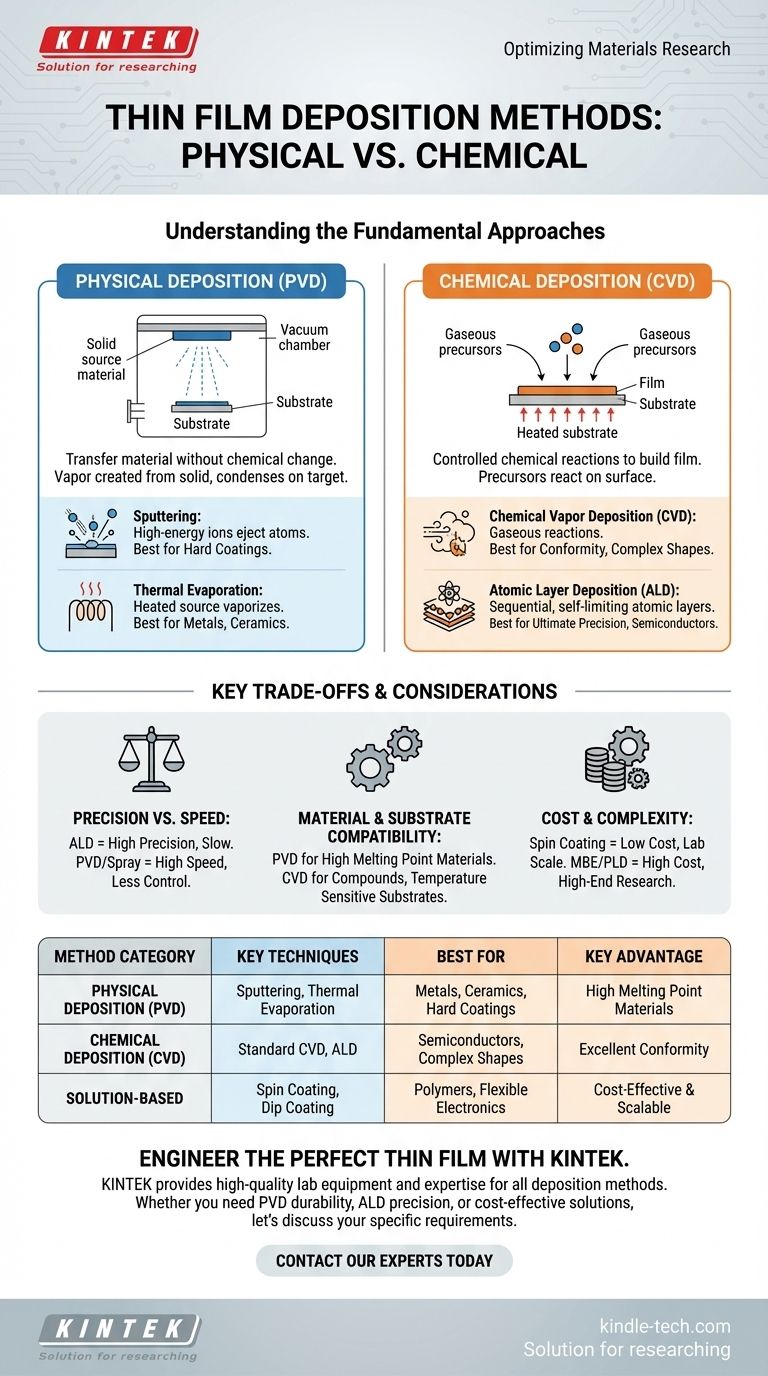
The Two Fundamental Approaches: Physical vs. Chemical
At the highest level, all deposition techniques are sorted by their underlying mechanism. This primary division informs everything from the equipment required to the types of materials that can be deposited.
Physical Deposition Methods
Physical methods transfer a material from a source to a substrate without altering its chemical composition. The process typically involves creating a vapor from a solid source material within a vacuum chamber, which then condenses onto the target surface.
Physical Vapor Deposition (PVD) is the umbrella term for these techniques. It is highly effective for depositing materials with high melting points, such as metals and ceramics, to create hard, wear-resistant coatings.
Two prominent PVD methods are sputtering, where high-energy ions bombard a source target to eject atoms that then deposit on the substrate, and thermal evaporation, where the source material is heated in a vacuum until it vaporizes and condenses on the substrate.
Chemical Deposition Methods
Chemical methods use controlled chemical reactions to create and deposit the thin film. Gaseous or liquid chemical precursors react on or near the substrate surface, leaving behind a solid layer of the desired material.
Chemical Vapor Deposition (CVD) is a cornerstone of this category. In CVD, the substrate is exposed to one or more volatile precursor gases, which react and decompose on the substrate surface to produce the desired film.
A highly advanced subset of this is Atomic Layer Deposition (ALD). This technique deposits a film one single atomic layer at a time through sequential, self-limiting chemical reactions, offering unparalleled precision and control over thickness and uniformity.
Other chemical methods include solution-based processes like spin coating and dip coating, which are often used for polymer compounds in applications like flexible electronics.
Understanding the Key Trade-offs
Selecting a deposition method involves balancing competing factors. There is no universally superior choice, only the most appropriate choice for a specific goal.
Precision vs. Speed
There is often an inverse relationship between deposition speed and film quality. Techniques like ALD offer atomic-level precision, creating perfectly uniform and conformal films, but the process is inherently slow.
Conversely, methods like sputtering (PVD) or spray pyrolysis can deposit material much more quickly over large areas but may offer less control over film conformity and microscopic structure.
Material and Substrate Compatibility
The material you wish to deposit is a primary constraint. PVD is excellent for metals, alloys, and ceramics that can be physically vaporized.
CVD relies on the availability of suitable precursor chemicals that can react to form the desired material, making it ideal for compounds like silicon dioxide or silicon nitride used in the semiconductor industry. The process temperature is also critical, as the substrate must be able to withstand the heat required for the chemical reaction.
Cost and Complexity
The complexity and cost of the required equipment vary dramatically. A simple spin coater is a relatively low-cost tool suitable for labs and prototyping.
In contrast, a system for Molecular Beam Epitaxy (MBE) or Pulsed Laser Deposition (PLD) represents a significant capital investment, reserved for high-end research and manufacturing where absolute purity and crystalline quality are non-negotiable.
Making the Right Choice for Your Application
Your final decision should be guided by the primary requirements of your project, whether it's performance, cost, or scale.
- If your primary focus is ultimate precision and conformity for semiconductors or optics: Your best options are likely Atomic Layer Deposition (ALD) or Molecular Beam Epitaxy (MBE).
- If your primary focus is a hard, durable coating for tools or automotive parts: Physical Vapor Deposition (PVD) techniques like sputtering are the industry standard.
- If your primary focus is coating complex, non-line-of-sight surfaces uniformly: Chemical Vapor Deposition (CVD) is often the superior choice due to the nature of gas-phase reactions.
- If your primary focus is cost-effective application of polymers or materials for flexible electronics: Solution-based methods like spin coating or spray pyrolysis provide a rapid and scalable path.
By understanding these fundamental categories and trade-offs, you can engineer materials with the precise properties your application demands.
Summary Table:
| Method Category | Key Techniques | Best For | Key Advantage |
|---|---|---|---|
| Physical Deposition (PVD) | Sputtering, Thermal Evaporation | Metals, Ceramics, Hard Coatings | High Melting Point Materials |
| Chemical Deposition (CVD) | Standard CVD, ALD | Semiconductors, Complex Shapes | Excellent Conformity |
| Solution-Based | Spin Coating, Dip Coating | Polymers, Flexible Electronics | Cost-Effective & Scalable |
Engineer the perfect thin film for your application with KINTEK.
Choosing the right deposition method is critical to achieving the material properties you need. Whether your project requires the durability of a PVD coating, the precision of ALD for semiconductors, or the cost-effectiveness of solution-based methods, KINTEK has the expertise and equipment to support your laboratory's success.
We specialize in providing high-quality lab equipment and consumables for all your thin film deposition needs. Let's discuss your specific requirements and find the optimal solution together.
Contact our experts today for a personalized consultation!
Visual Guide
Related Products
- Aluminized Ceramic Evaporation Boat for Thin Film Deposition
- Tungsten Evaporation Boat for Thin Film Deposition
- Electron Beam Evaporation Coating Oxygen-Free Copper Crucible and Evaporation Boat
- Molybdenum Tungsten Tantalum Evaporation Boat for High Temperature Applications
- HFCVD Machine System Equipment for Drawing Die Nano-Diamond Coating
People Also Ask
- Why is an alumina boat and Ti3AlC2 powder bed necessary for Ti2AlC sintering? Protect MAX Phase Purity
- What is the source of evaporation for thin film? Choosing Between Thermal and E-Beam Methods
- What is the widely used boat made of in thermal evaporation? Choosing the Right Material for High-Purity Deposition
- What is thin film deposition? Unlock Advanced Surface Engineering for Your Materials
- Why are high-purity ceramic boats used for lignin activation? Ensure Purity & Thermal Stability


