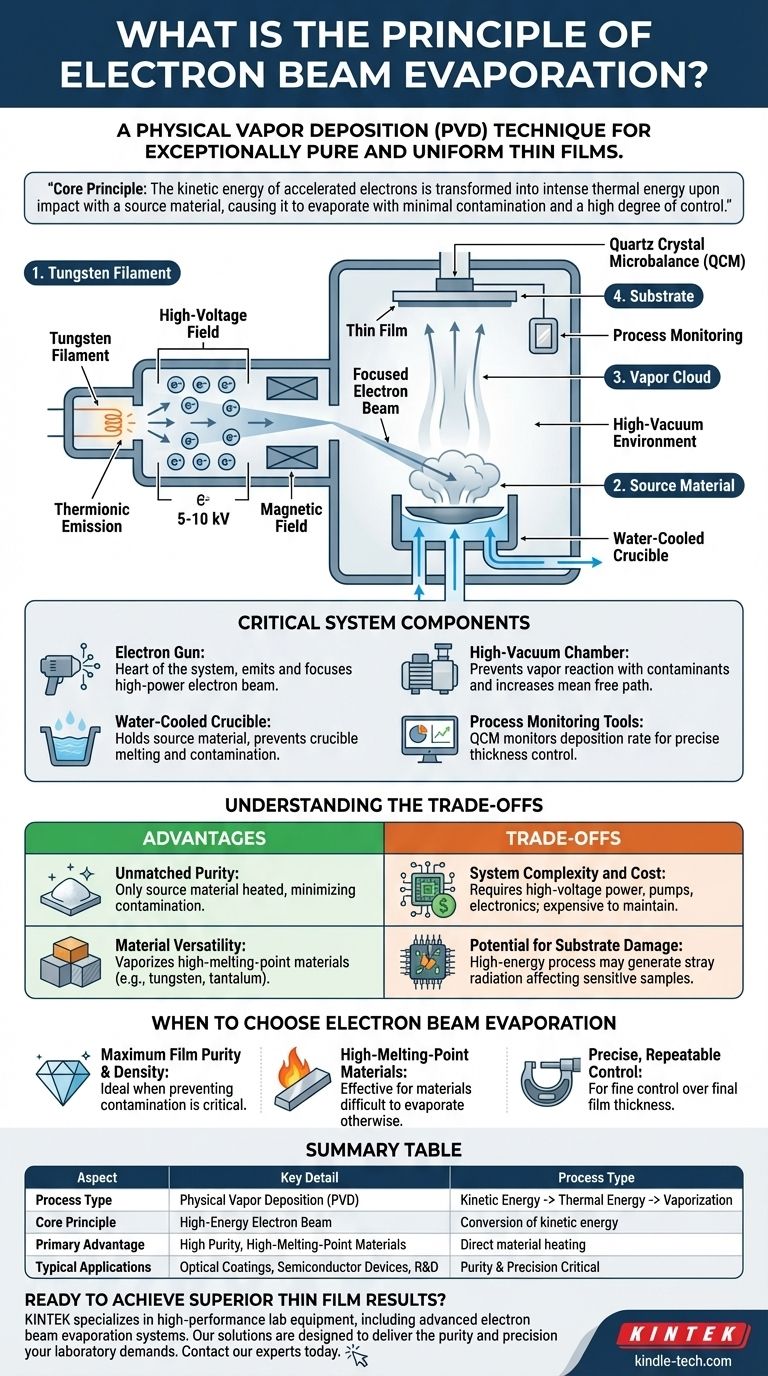
In short, electron beam evaporation is a physical vapor deposition (PVD) technique that uses a focused beam of high-energy electrons to vaporize a source material. This vapor then travels through a high-vacuum chamber and condenses onto a cooler surface, or substrate, to form an exceptionally pure and uniform thin film.
The core principle is the targeted conversion of energy. The kinetic energy of accelerated electrons is transformed into intense thermal energy upon impact with a source material, causing it to evaporate with minimal contamination and a high degree of control.
How It Works: A Step-by-Step Breakdown
The entire process is a carefully orchestrated sequence designed for precision and purity, all occurring within a high-vacuum environment.
Generation: Creating the Electron Beam
The process begins with a tungsten filament. A high electrical current is passed through this filament, causing it to heat up significantly through a process known as joule heating.
This intense heat causes the filament to release electrons via thermionic emission.
Acceleration and Focusing: Forming a High-Energy Beam
Once freed, the electrons are accelerated by a high-voltage field, typically between 5 and 10 kilovolts (kV), giving them immense kinetic energy.
A magnetic field is then used to precisely focus these high-speed electrons into a narrow, controllable beam.
Impact and Vaporization: The Energy Transfer
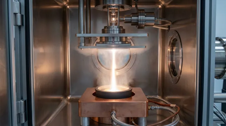
This focused electron beam is directed onto the source material, which is held in a crucible. Upon striking the material, the electrons' kinetic energy is instantly converted into intense, localized heat.
This energy transfer raises the material's temperature past its boiling point, causing it to evaporate (or sublimate, for some materials), creating a vapor cloud.
Deposition: From Vapor to Solid Film
The vaporized material travels upward through the vacuum chamber. The vacuum is critical, as it ensures the vapor particles travel in a straight line without colliding with or reacting to air molecules.
When the vapor reaches the cooler substrate positioned above the source, it condenses, forming a thin, solid film. The thickness of this film, often between 5 and 250 nanometers, can be precisely controlled.
The Critical System Components
Understanding the key hardware reveals why this technique is so effective and controllable.
The Electron Gun
This is the heart of the system, comprising the tungsten filament that emits electrons and the electromagnetic lenses that accelerate and focus them into a high-power beam.
The Water-Cooled Crucible
The source material is held in a copper crucible that is actively water-cooled. This is a crucial design feature.
By cooling the crucible, only the small spot hit by the electron beam is heated. This prevents the crucible itself from melting or outgassing, which would otherwise contaminate the resulting film.
The High-Vacuum Chamber
The chamber maintains an extremely low-pressure environment. This serves two purposes: it prevents the vaporized material from reacting with contaminants like oxygen, and it increases the "mean free path" so vapor atoms travel directly to the substrate without interference.
Process Monitoring Tools
Systems almost always include a quartz crystal microbalance (QCM). This device monitors the rate of deposition in real-time, allowing for precise control over the final film thickness.
Understanding the Trade-offs
No technique is perfect for every application. E-beam evaporation offers significant advantages but comes with inherent complexities.
Advantage: Unmatched Purity
Because only the source material is heated, contamination from the container is virtually eliminated. This results in films of exceptionally high purity, which is critical for optical and electronic applications.
Advantage: Material Versatility
The intense, focused energy can vaporize materials with very high melting points, such as refractory metals (tungsten, tantalum) and ceramics, that are impossible to evaporate with simpler thermal heating methods.
Trade-off: System Complexity and Cost
E-beam evaporators are mechanically complex. They require high-voltage power supplies, powerful vacuum pumps, and sophisticated control electronics, making them more expensive to purchase and maintain than other deposition systems.
Trade-off: Potential for Substrate Damage
The high-energy process can generate stray electrons and X-rays. For highly sensitive substrates, such as certain organic electronics or biological samples, this secondary radiation can cause damage.
When to Choose Electron Beam Evaporation
Your application's requirements for purity, material type, and control will determine if this method is the right choice.
- If your primary focus is maximum film purity and density: E-beam is the superior choice because direct heating of the source material prevents contamination from the crucible.
- If you need to deposit materials with very high melting points: The intense, localized heating of the electron beam makes it one of the few effective and reliable options available.
- If your goal is precise, repeatable control over film thickness: The integration of real-time monitoring tools like a QCM allows for exceptionally fine control over the final film properties.
Ultimately, electron beam evaporation is the industry standard when the performance, purity, and precision of the thin film are non-negotiable.
Summary Table:
| Aspect | Key Detail |
|---|---|
| Process Type | Physical Vapor Deposition (PVD) |
| Core Principle | Kinetic energy from an electron beam is converted to thermal energy to vaporize a source material. |
| Primary Advantage | Exceptionally high film purity and the ability to deposit high-melting-point materials. |
| Typical Applications | Optical coatings, semiconductor devices, and demanding R&D. |
Ready to achieve superior thin film results? KINTEK specializes in high-performance lab equipment, including advanced electron beam evaporation systems. Our solutions are designed to deliver the purity and precision your laboratory demands. Contact our experts today to discuss how we can support your specific application needs.
Visual Guide
Related Products
- Electron Beam Evaporation Coating Tungsten Crucible and Molybdenum Crucible for High Temperature Applications
- Electron Beam Evaporation Coating Oxygen-Free Copper Crucible and Evaporation Boat
- Electron Beam Evaporation Coating Gold Plating Tungsten Molybdenum Crucible for Evaporation
- Electron Beam Evaporation Coating Conductive Boron Nitride Crucible BN Crucible
- E Beam Crucibles Electron Gun Beam Crucible for Evaporation
People Also Ask
- What is the current of e-beam evaporation? A Guide to High-Purity Thin Film Deposition
- What is the deposition rate of e-beam evaporation? Control Thin Film Quality and Speed
- What is the container that holds the metal source material called in e-beam evaporation? Ensure Purity and Quality in Your Thin-Film Deposition
- What is e-beam evaporation? Achieve High-Purity Thin Film Deposition for Your Lab
- What materials are used in electron beam evaporation? Master High-Purity Thin Film Deposition


