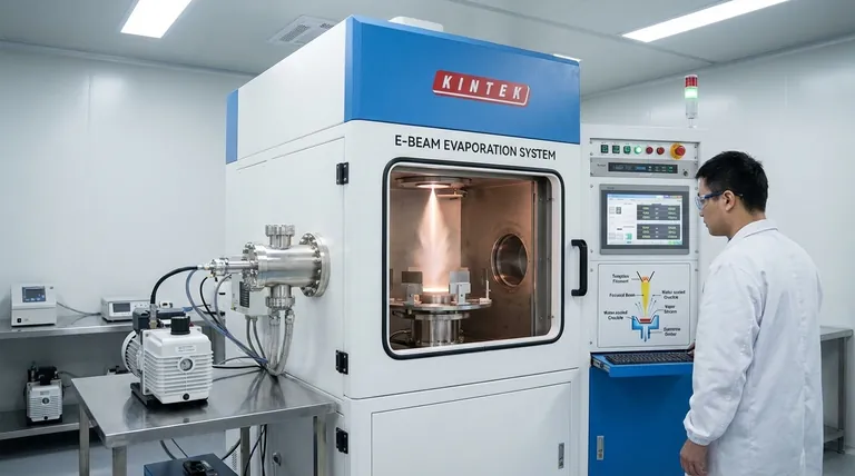
Electron Beam (E-Beam) Evaporation is a high-vacuum Physical Vapor Deposition (PVD) technique used to create exceptionally thin and pure coatings. The process uses a focused, high-energy beam of electrons to heat a source material, causing it to vaporize. This vapor then travels in a straight line and condenses onto a substrate, forming a precise, atom-by-atom film.
E-beam coating is fundamentally a line-of-sight deposition process prized for its precision and low thermal impact on the component being coated. It excels at creating extremely pure, dense films for specialized applications, but its directional nature presents challenges for coating complex, three-dimensional geometries.
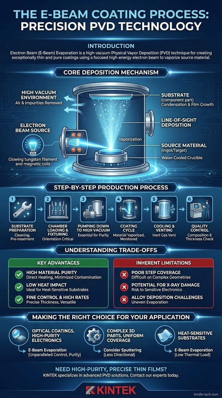
The Core Deposition Mechanism
To understand the e-beam process, it is essential to grasp the core physics that take place inside the vacuum chamber. Each step is precisely controlled to achieve a specific film composition and thickness.
The Vacuum Environment
The entire process occurs within a high-vacuum chamber. Evacuating the chamber is critical to remove air and other gaseous impurities that could otherwise react with the vaporized material and contaminate the final film. This near-vacuum state also allows vapor atoms to travel directly to the substrate without colliding with other particles.
The Electron Beam Source
A tungsten filament is heated to generate a stream of electrons. These electrons are then accelerated and focused into a high-energy beam using a series of magnetic fields, similar to the way a cathode-ray tube (CRT) television works.
Vaporizing the Source Material
This focused electron beam is directed onto the source material (often called an ingot or target), which is held in a water-cooled copper crucible. The intense energy from the beam heats the material to its boiling point, causing it to evaporate or sublimate into a vapor.
Line-of-Sight Deposition
The atoms of vapor travel in a straight, direct path from the source to the substrate. This "line-of-sight" characteristic means the coating only deposits on surfaces that are directly visible from the evaporation source.
Condensation and Film Growth
When the vapor atoms reach the comparatively cool surface of the substrate, they condense. This process builds the coating layer by layer, atom by atom, resulting in a very fine-grained and dense thin film.
The Step-by-Step Production Process
Moving from the core mechanism to an industrial application involves a series of carefully managed production steps.
Step 1: Substrate Preparation
Proper adhesion is impossible without a pristine surface. This step involves rigorous cleaning to remove any contaminants. Depending on the part's history, it may also include stripping old coatings or specific pre-treatments to prepare the surface.
Step 2: Chamber Loading and Fixturing
The source material is placed in its crucible, and the substrates are mounted on specialized fixtures or holders. The orientation of these fixtures is critical due to the line-of-sight nature of the process, ensuring the target surfaces are correctly exposed to the vapor stream.
Step 3: Pumping Down to High Vacuum
Once loaded, the chamber is sealed and evacuated to a target pressure level. This pump-down can take a significant amount of time but is essential for the purity of the final coating.
Step 4: The Coating Cycle
With the vacuum established, the electron beam is activated, and the material is vaporized. The deposition rate and final thickness are monitored in real-time to ensure the film meets precise specifications. The entire cycle can range from thirty minutes to several hours depending on the material and desired thickness.
Step 5: Cooling and Venting
After the target thickness is reached, the electron beam is deactivated. The system is allowed to cool before the chamber is vented with an inert gas, returning it to atmospheric pressure.
Step 6: Quality Control
Each batch undergoes rigorous inspection. Technicians use tools like an X-ray fluorescent (XRF) machine to verify the coating's composition and thickness, ensuring it meets all required standards.
Understanding the Trade-offs
No single coating technology is perfect for every application. E-beam evaporation has distinct advantages and limitations that define its ideal use cases.
Key Advantages
- High Material Purity: The electron beam directly heats only the source material, not the entire crucible, minimizing contamination and resulting in exceptionally pure films.
- Low Heat Impact: The process transfers less heat to the substrate compared to other methods, making it ideal for coating heat-sensitive materials like plastics, polymers, or pre-assembled electronic components.
- Fine Control & High Rates: It allows for very precise control over deposition rate and film thickness while also being capable of achieving very high evaporation rates for a wide range of materials, including metals and ceramics.
Inherent Limitations
- Poor Step Coverage: The highly directional vapor stream makes it difficult to uniformly coat complex shapes, sharp edges, or internal surfaces. It primarily coats what it can "see."
- Potential for X-Ray Damage: The interaction of high-energy electrons with the source material can generate X-rays. While typically low-level, these can be sufficient to damage highly sensitive electronic substrates or optical components.
- Alloy Deposition Challenges: It can be difficult to evaporate materials made of multiple elements (alloys) with different vapor pressures, as the more volatile element will evaporate first.
Making the Right Choice for Your Application
Selecting the correct PVD method requires aligning the process capabilities with your primary engineering goal.
- If your primary focus is optical coatings or high-purity electronics: E-beam evaporation offers unparalleled control over film thickness, purity, and density, which is critical for these applications.
- If your primary focus is coating complex 3D parts with uniform coverage: You should consider less directional PVD methods like sputtering to ensure all surfaces are adequately coated.
- If your primary focus is coating heat-sensitive substrates: The low thermal load of the e-beam process makes it a superior choice for protecting materials like polymers or delicate, pre-assembled components.
Ultimately, selecting e-beam evaporation is a strategic decision for applications where the final film quality and precision are more critical than achieving uniform geometric coverage.
Summary Table:
| Key Aspect | Details |
|---|---|
| Process Type | Physical Vapor Deposition (PVD) |
| Environment | High Vacuum |
| Mechanism | Line-of-Sight Deposition |
| Key Advantages | High Purity, Low Thermal Impact, Precise Thickness Control |
| Ideal For | Optical Coatings, High-Purity Electronics, Heat-Sensitive Substrates |
| Limitations | Poor Coverage on Complex 3D Geometries |
Need high-purity, precise thin films for your research or production?
KINTEK specializes in advanced lab equipment, including PVD solutions for demanding applications. Our expertise can help you select the right coating technology to ensure superior film quality, purity, and performance for your specific substrates and goals.
Contact our experts today to discuss how we can support your laboratory's thin-film deposition needs.
Visual Guide
Related Products
- Electron Beam Evaporation Coating Tungsten Crucible and Molybdenum Crucible for High Temperature Applications
- Electron Beam Evaporation Coating Conductive Boron Nitride Crucible BN Crucible
- Electron Beam Evaporation Coating Gold Plating Tungsten Molybdenum Crucible for Evaporation
- Electron Beam Evaporation Coating Oxygen-Free Copper Crucible and Evaporation Boat
- High Purity Pure Graphite Crucible for Electron Beam Evaporation
People Also Ask
- What is e-beam evaporation? Achieve High-Purity Thin Film Deposition for Your Lab
- What is e-beam evaporation used for? Precision Coating for Optics, Aerospace & Electronics
- What is the voltage of e-beam evaporation? Achieve Precise Thin-Film Deposition
- What materials are used in electron beam evaporation? Master High-Purity Thin Film Deposition
- What is the container that holds the metal source material called in e-beam evaporation? Ensure Purity and Quality in Your Thin-Film Deposition


