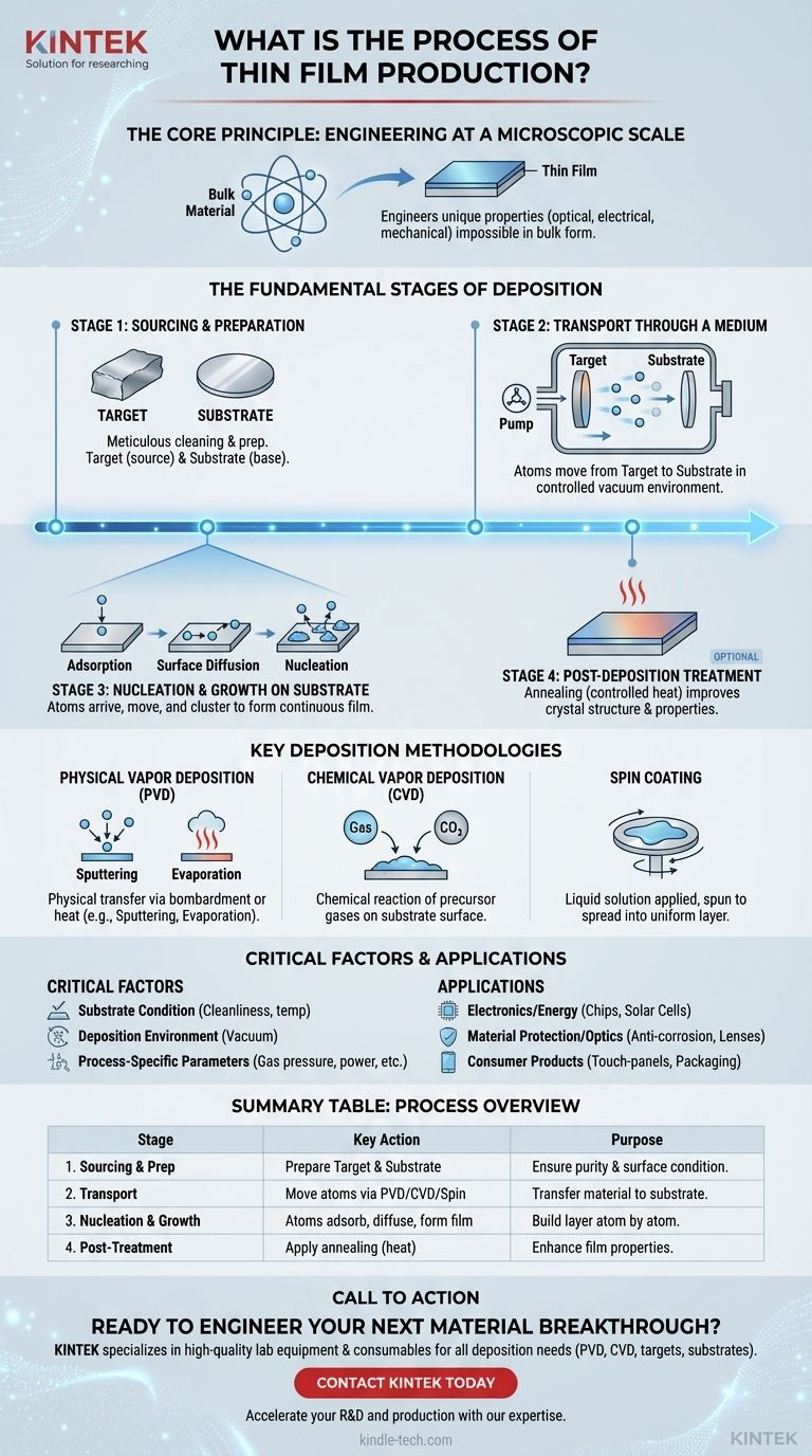
In essence, the production of a thin film is a highly controlled process where a source material, known as a target, is transported through a medium like a vacuum and deposited atom by atom onto a surface, called a substrate. This process typically involves preparing the source material and substrate, executing the deposition using a specific technique, and sometimes applying post-treatment like heating to refine the film's final properties.
The core principle is not simply to coat a surface, but to engineer a new material at a microscopic scale. By controlling the deposition process with extreme precision, we can create films with unique optical, electrical, and mechanical properties that are impossible to achieve in the material's bulk form.
The Fundamental Stages of Deposition
The creation of a thin film can be broken down into a series of fundamental, sequential stages. Each step is critical for achieving the desired thickness, composition, and overall quality of the final layer.
Stage 1: Sourcing and Preparation
Before deposition can begin, both the source material and the destination surface must be meticulously prepared.
The target is the pure source material—whether a metal, alloy, or polymer—that will form the film. The substrate is the base material (like a silicon wafer or glass panel) onto which the film will be grown.
Stage 2: Transport Through a Medium
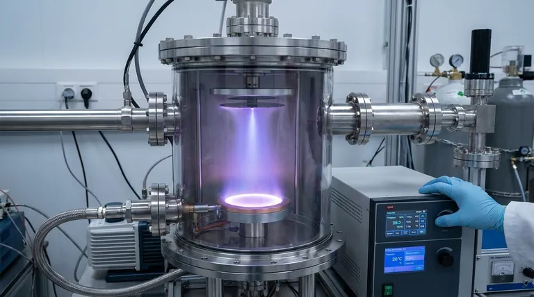
The next step is to move atoms or molecules from the target to the substrate. This is the defining stage of the process and is accomplished using a variety of techniques within a controlled environment, often a vacuum chamber.
This transport mechanism is what distinguishes the primary methods of thin film production.
Stage 3: Nucleation and Growth on the Substrate
The film does not simply appear fully formed. It grows through a complex physical process on the substrate's surface.
This growth is governed by three key phenomena:
- Adsorption: Atoms from the source material arrive and attach to the substrate surface.
- Surface Diffusion: These newly arrived atoms move around on the surface, finding energetically favorable spots.
- Nucleation: Atoms cluster together to form stable "islands," which then grow and coalesce to create a continuous film.
Stage 4: Post-Deposition Treatment (Optional)
In some cases, the film is subjected to additional processes after deposition to enhance its properties.
Annealing, or controlled heat treatment, is a common method used to improve the film's crystal structure, reduce internal stress, and optimize its electrical or optical performance.
Key Deposition Methodologies
While the fundamental stages are universal, the method used for the "Transport" stage has a significant impact on the film's characteristics. The most common families of techniques are Physical Vapor Deposition, Chemical Vapor Deposition, and liquid-phase coating.
Physical Vapor Deposition (PVD)
PVD methods use physical mechanisms like high-energy bombardment or heating to transfer material.
Sputtering involves bombarding the target with energized ions, which ejects atoms that then travel and deposit onto the substrate. Evaporation uses heat to vaporize the target material within a vacuum, allowing the vapor to condense onto the cooler substrate.
Chemical Vapor Deposition (CVD)
CVD is a chemical process where the substrate is exposed to volatile precursor gases. These gases react or decompose on the substrate's surface, leaving behind the desired solid material as a thin film.
Spin Coating
This method is common for polymer films and starts with a liquid solution. A small amount of the material dissolved in a solvent is applied to the center of the substrate, which is then spun at high speed to spread the liquid into an extremely thin, uniform layer as the solvent evaporates.
Understanding the Trade-offs and Critical Factors
The success of any thin film process hinges on precise control over numerous variables. A failure to manage these factors can result in a film that is non-uniform, poorly adhered, or lacks the required properties.
The Substrate's Condition
The cleanliness, smoothness, and temperature of the substrate are paramount. Any contamination can prevent proper film adhesion and growth, leading to defects.
The Deposition Environment
Most high-performance films are deposited in a vacuum. This is critical to prevent atoms from the source material from colliding with air molecules and to avoid unwanted chemical reactions with oxygen or nitrogen.
Process-Specific Parameters
Each deposition method has its own set of critical variables. For spin coating, these include the solution's concentration, the solvent's boiling point, and the spinning rate and duration. For sputtering, factors like gas pressure and power levels are key.
Making the Right Choice for Your Application
The specific method and parameters chosen are entirely dictated by the intended application of the thin film. The technology's versatility is what makes it a cornerstone of modern industry.
- If your primary focus is electronics and energy: The precision of CVD and PVD is essential for building the microscopic layered structures found in semiconductor chips, solar cells, and thin-film batteries.
- If your primary focus is material protection and optics: Thin films are used to create durable, anti-corrosion coatings on machine parts, wear-resistant layers on tools, and multi-layered anti-reflective coatings on eyeglass lenses.
- If your primary focus is consumer products: The applications are vast, from the decorative and protective coatings on bathroom fittings to the metallic layers inside food packaging that preserve freshness and the conductive films that enable touch-panel displays.
By manipulating materials at the atomic level, thin film production enables the creation of technologies that would otherwise be impossible.
Summary Table:
| Stage | Key Action | Purpose |
|---|---|---|
| 1. Sourcing & Preparation | Prepare target material and substrate (e.g., silicon wafer) | Ensure purity and proper surface for deposition |
| 2. Transport | Move atoms/molecules via PVD, CVD, or spin coating in a controlled environment | Transfer material to the substrate |
| 3. Nucleation & Growth | Atoms adsorb, diffuse, and form a continuous film on the substrate | Build the thin film layer atom by atom |
| 4. Post-Treatment (Optional) | Apply annealing (heat treatment) | Enhance film properties like structure and conductivity |
Ready to Engineer Your Next Material Breakthrough?
The precise control required for successful thin film production demands reliable equipment and expert support. At KINTEK, we specialize in providing high-quality lab equipment and consumables for all your deposition needs—from robust PVD and CVD systems to substrates and targets.
Whether you're developing advanced semiconductors, protective coatings, or next-generation optics, our solutions are designed to help you achieve superior film quality and consistency.
Contact KINTEK today to discuss your specific application and discover how our expertise can accelerate your R&D and production processes.
Visual Guide
Related Products
- Vacuum Hot Press Furnace Machine for Lamination and Heating
- Lab Blown Film Extrusion Three Layer Co-Extrusion Film Blowing Machine
- Lab Plastic PVC Calender Stretch Film Casting Machine for Film Testing
People Also Ask
- What role does mechanical pressure play during the vacuum diffusion bonding of tungsten and copper? Keys to Solid Bonding
- What advantages does a vacuum hot press furnace provide for LSLBO ceramic electrolytes? Achieve 94% Relative Density
- How does the vacuum system within a vacuum hot press furnace contribute to the quality of aluminum matrix composites?
- Why is it necessary to maintain a high-vacuum environment within a vacuum hot press furnace? Optimize Cu-SiC Sintering
- What are the advantages of a vacuum hot press furnace for W-50%Cu? Achieve 99.6% Density at Lower Temperatures


