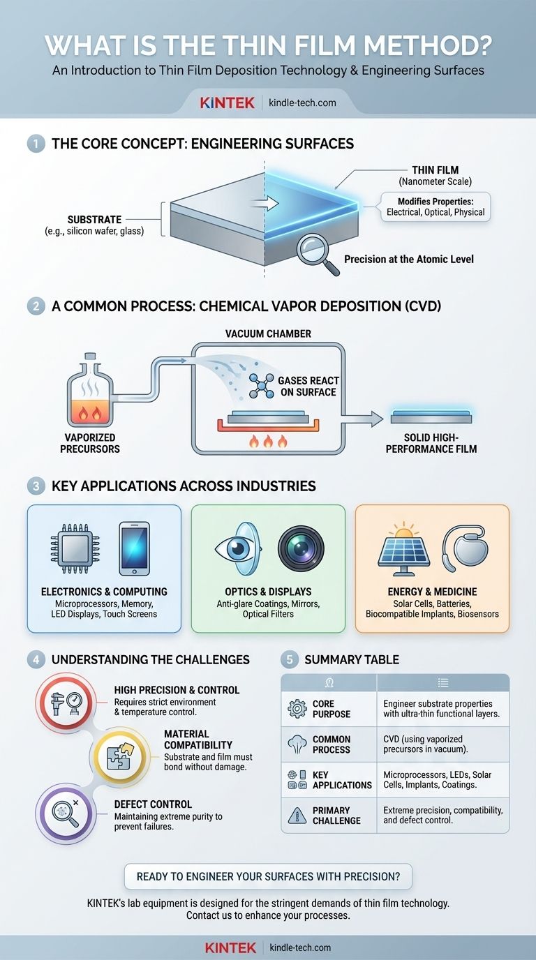
In essence, the 'thin film method' refers to a set of advanced manufacturing processes known as thin film deposition. These techniques are used to apply an extremely thin layer of material—often only a few atoms or molecules thick—onto a surface called a substrate. By precisely controlling the thickness and composition of this film, we can fundamentally alter the substrate's physical, optical, or electrical properties to achieve a specific function.
The core purpose of thin film deposition is not to simply coat a surface, but to engineer its properties with microscopic precision. This foundational technology is what enables the high performance of modern devices, from the anti-glare on your glasses to the complex circuitry inside your smartphone.
The Fundamental Goal of Thin Film Deposition
At its heart, this technology is about giving a material new capabilities it doesn't naturally possess. The process involves adding a functional layer to a base material, creating a composite with enhanced characteristics.
Modifying a Substrate's Surface
The process always starts with a substrate, which is the base material being coated. This could be a silicon wafer, a piece of glass for a lens, or a medical implant.
The goal is to deposit a thin film onto this substrate. This film imparts a new property, such as electrical conductivity, insulation, reflectivity, or hardness, that the substrate lacks on its own.
Achieving Microscopic Precision
The term "thin" is critical. These films are engineered on a nanometer scale, allowing for the extreme miniaturization required for modern electronics and other advanced systems.
This precision is what allows engineers to build the intricate, multi-layered structures found in microprocessors, solar cells, and high-performance optical lenses.
A Common Process: Chemical Vapor Deposition (CVD)
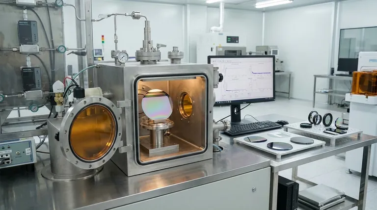
One of the most common thin film methods is Chemical Vapor Deposition (CVD). In this process, a substrate is placed in a vacuum chamber.
Two or more chemical precursors are heated until they vaporize. When these gases meet on the surface of the substrate, they react chemically to form a solid, high-performance thin film.
Where This Technology is Used
The applications of thin film deposition are vast and integral to nearly every field of modern technology. The ability to engineer surfaces at this scale is a cornerstone of innovation.
In Electronics and Computing
Thin films are the building blocks of the digital world. They are used to create the transistor arrays in microprocessors, the magnetic films for computer memory, and the conductive and insulating layers in semiconductor devices.
The technology is also essential for manufacturing LED displays and the transparent conductive layers used in touch screens for phones and tablets.
In Optics and Displays
Nearly all advanced optical components rely on thin film coatings. These layers are applied to lenses and glass to improve light transmission, control reflection (as in anti-glare coatings), and manage refraction.
The silvering on a mirror is a classic example of a thin film, as are the specialized coatings that filter specific wavelengths of light.
In Energy and Medicine
Thin film deposition is critical for next-generation energy and medical solutions. It is used to manufacture advanced solar cells that efficiently convert light into electricity and to create new types of batteries.
In the biomedical field, thin films are applied to medical implants to ensure they are biocompatible and to create sophisticated drug delivery systems and biosensors.
Understanding the Challenges
While incredibly powerful, thin film deposition is a highly specialized process. Understanding its inherent complexities is key to appreciating its value.
High Precision Requires High Control
Depositing a film that is perfectly uniform and only a few atoms thick requires an extremely controlled environment. Processes like CVD require vacuum chambers and precise temperature control, making the equipment complex and expensive.
Material Compatibility is Key
The chemical and physical properties of both the substrate and the film material must be compatible. The film must adhere properly to the substrate and withstand the conditions of the deposition process without being damaged.
Defect Control is a Constant Battle
At the microscopic scale, even a single speck of dust or a minor impurity can create a defect that ruins a device. Maintaining purity and preventing defects is a major engineering challenge, especially in semiconductor manufacturing.
How to Think About Thin Film Applications
To apply this knowledge, consider the core function you are trying to achieve.
- If your primary focus is electronics: Think of thin films as the microscopic "wiring" and "switches" that create integrated circuits and displays.
- If your primary focus is optics: See these films as engineered layers that precisely manipulate how light behaves, creating anti-reflective lenses or perfect mirrors.
- If your primary focus is material science: View thin film deposition as a fundamental tool for designing entirely new surface properties for applications like solar cells or durable coatings.
Ultimately, thin film deposition is the art of engineering surfaces at the atomic level, making it a foundational process for virtually all advanced technology.
Summary Table:
| Key Aspect | Description |
|---|---|
| Core Purpose | To engineer a substrate's properties by applying an ultra-thin functional layer. |
| Common Process | Chemical Vapor Deposition (CVD), using vaporized precursors in a vacuum chamber. |
| Key Applications | Microprocessors, LED displays, solar cells, medical implants, optical coatings. |
| Primary Challenge | Requires extreme precision, material compatibility, and stringent defect control. |
Ready to engineer your surfaces with precision?
Thin film deposition is a complex process that requires specialized equipment and expertise. Whether you are developing advanced semiconductors, optical components, or medical devices, KINTEK's lab equipment and consumables are designed to meet the stringent demands of thin film technology.
We provide the reliable tools you need to achieve high-purity, uniform coatings and drive your innovations forward.
Contact KINTEK today to discuss your specific laboratory requirements and discover how our solutions can enhance your thin film processes.
Visual Guide
Related Products
- Aluminized Ceramic Evaporation Boat for Thin Film Deposition
- Tungsten Evaporation Boat for Thin Film Deposition
- Electron Beam Evaporation Coating Oxygen-Free Copper Crucible and Evaporation Boat
- Molybdenum Tungsten Tantalum Evaporation Boat for High Temperature Applications
- HFCVD Machine System Equipment for Drawing Die Nano-Diamond Coating
People Also Ask
- What is the widely used boat made of in thermal evaporation? Choosing the Right Material for High-Purity Deposition
- What are the alternatives to sputtering? Choose the Right Thin Film Deposition Method
- Why are high-purity ceramic boats used for lignin activation? Ensure Purity & Thermal Stability
- What are thin films deposited by evaporation? A Guide to High-Purity Coating
- What is the source of evaporation for thin film? Choosing Between Thermal and E-Beam Methods


