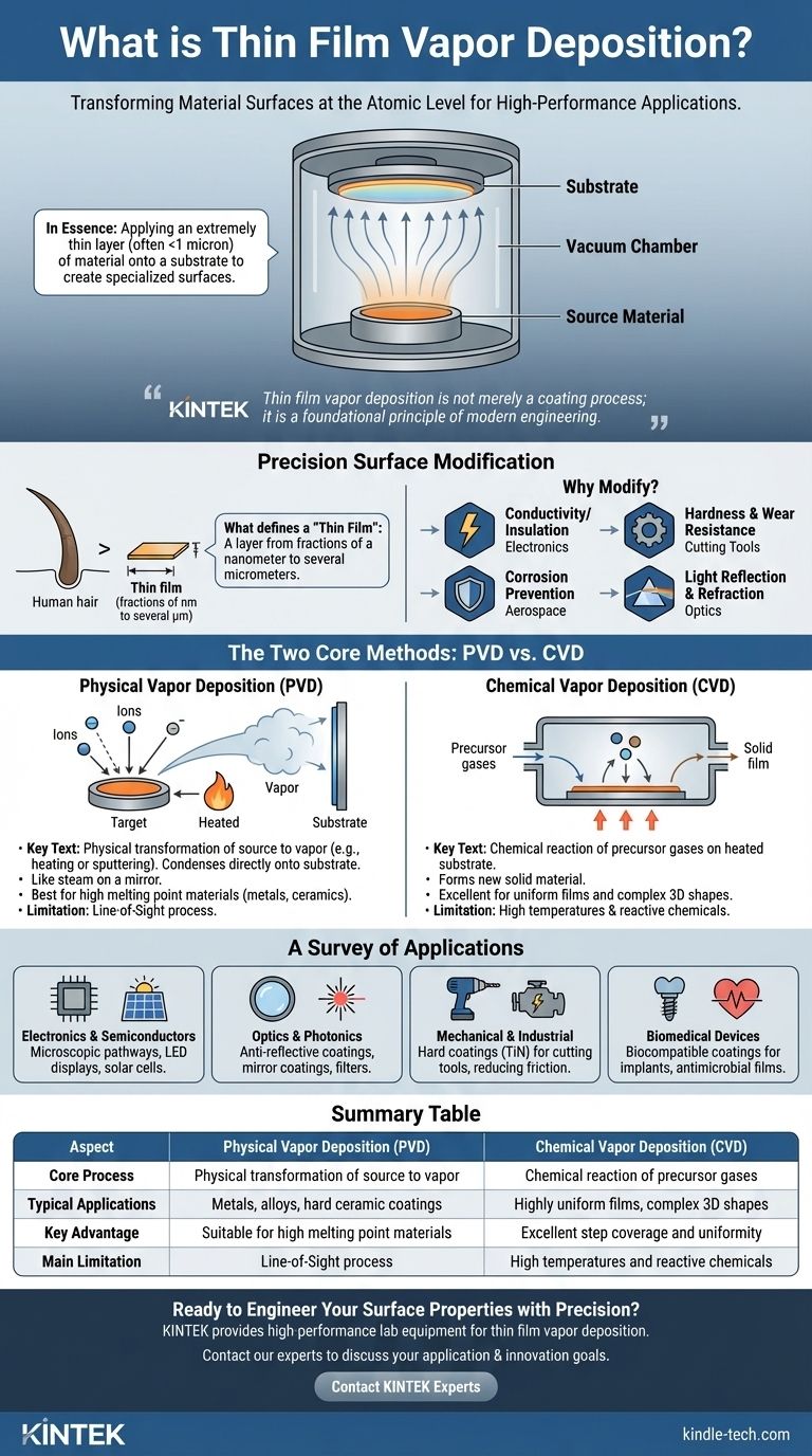
In essence, thin film vapor deposition is a family of manufacturing techniques used to apply an extremely thin layer of material—often less than a single micron thick—onto a surface, known as a substrate. The process involves converting a source material into a vapor within a vacuum, which then travels and settles onto the substrate, forming a solid, high-performance film. This method is fundamental to creating the specialized surfaces that power modern technology.
Thin film vapor deposition is not merely a coating process; it is a foundational principle of modern engineering. It allows us to fundamentally alter the properties of a material's surface, enabling the creation of everything from faster microchips to more durable mechanical parts.
The Fundamental Goal: Precision Surface Modification
At its core, vapor deposition is about changing how the surface of an object behaves. The goal is to add new properties that the original material lacks.
What Defines a "Thin Film"
A "thin film" is a layer of material ranging in thickness from fractions of a nanometer to several micrometers. For context, a human hair is about 70 micrometers thick.
This precise control over thickness and composition allows engineers to imbue a surface with specific electrical, optical, or mechanical properties.
Why Modify a Surface?
Depositing a thin film can radically change a material's characteristics. The specific goal depends entirely on the application.
Common modifications include improving conductivity or insulation for electronics, increasing hardness and wear resistance for cutting tools, preventing corrosion on aerospace components, or managing the reflection and refraction of light for optical lenses.
The Two Core Methods: PVD vs. CVD
Vapor deposition is broadly divided into two main categories: Physical Vapor Deposition (PVD) and Chemical Vapor Deposition (CVD). The choice between them depends on the material being deposited and the desired outcome.
Physical Vapor Deposition (PVD)
In PVD, the source material is physically transformed into a vapor. This is typically done by heating it to its boiling point or by bombarding it with ions in a process called sputter deposition.
This vapor then travels through the vacuum chamber and condenses directly onto the cooler substrate, forming a solid film. Think of it like steam from boiling water condensing on a cold mirror. PVD is well-suited for depositing materials with high melting points, like pure metals and certain ceramics.
Chemical Vapor Deposition (CVD)
In CVD, the process relies on a chemical reaction. Precursor gases are introduced into the chamber, and when they come into contact with the heated substrate, they react with each other.
This reaction forms a new solid material that deposits onto the substrate as the thin film. CVD is highly effective for creating very pure, uniform films and for coating complex shapes, as the gases can reach all surfaces.
Where This Technology Is Used: A Survey of Applications
The ability to engineer surfaces at the atomic level makes thin film deposition a critical process across numerous high-tech industries.
Electronics and Semiconductors
This is perhaps the most well-known application. Thin films are used to create the microscopic conductive and insulating pathways in semiconductor devices, microchips, and integrated circuits. It is also essential for manufacturing LED displays, solar cells, and data storage devices.
Optics and Photonics
Optical coatings improve the performance of lenses and glass by controlling how they transmit or reflect light. This includes anti-reflective coatings on eyeglasses, mirror coatings, and specialized filters used in lasers and scientific instruments.
Mechanical and Industrial Components
Hard coatings made from materials like titanium nitride are deposited on cutting tools, drill bits, and engine parts to dramatically increase their hardness, reduce friction, and improve wear resistance. This extends component lifetime and boosts performance.
Biomedical Devices
Thin films are critical for medical implants like artificial joints or pacemakers. Biocompatible coatings ensure the body does not reject the device, while other films can add antimicrobial properties or improve durability.
Understanding the Trade-offs
While powerful, these techniques have inherent limitations that guide their use.
PVD: The Line-of-Sight Limitation
Because PVD involves a physical stream of vapor traveling from a source to a substrate, it is largely a "line-of-sight" process. It can be challenging to achieve a uniform coating on complex, three-dimensional objects with hidden surfaces or sharp angles.
CVD: Thermal and Chemical Constraints
CVD often requires very high temperatures to initiate the chemical reaction. The substrate must be able to withstand this heat without being damaged or warped. Furthermore, the precursor chemicals can be highly toxic, corrosive, or expensive, requiring specialized handling and equipment.
Overall Complexity and Cost
Both PVD and CVD systems are sophisticated and require significant capital investment. They operate in high-vacuum environments and demand precise control over temperature, pressure, and gas flow, making them best suited for high-value applications where performance is critical.
Making the Right Choice for Your Goal
The decision between PVD and CVD is driven by the material, the substrate, and the application's specific requirements.
- If your primary focus is depositing pure metals, alloys, or very hard ceramic coatings: PVD is often the more direct method, especially for materials with high melting points.
- If your primary focus is creating a highly uniform, pure film on a complex 3D shape: CVD's gas-based process is superior at coating intricate surfaces evenly.
- If your primary focus is modifying a surface property like conductivity or corrosion resistance: Both methods are viable, and the choice will depend on which process is more compatible with your specific substrate and coating materials.
Ultimately, understanding the distinction between these deposition methods is the key to successfully leveraging surface engineering for your specific goal.
Summary Table:
| Aspect | Physical Vapor Deposition (PVD) | Chemical Vapor Deposition (CVD) |
|---|---|---|
| Core Process | Physical transformation of source material into vapor | Chemical reaction of precursor gases on the substrate |
| Typical Applications | Metals, alloys, hard ceramic coatings | Highly uniform films, complex 3D shapes |
| Key Advantage | Suitable for high melting point materials | Excellent step coverage and uniformity |
| Main Limitation | Line-of-sight process | High temperatures and reactive chemicals |
Ready to Engineer Your Surface Properties with Precision?
Whether you are developing advanced semiconductors, durable industrial components, or specialized optical coatings, choosing the right deposition method is critical. KINTEK specializes in providing high-performance lab equipment and consumables for thin film vapor deposition processes, serving the precise needs of R&D and manufacturing laboratories.
Let our expertise help you select the ideal solution to enhance conductivity, hardness, or optical performance. Contact our experts today to discuss your specific application and discover how we can support your innovation goals.
Visual Guide
Related Products
- Aluminized Ceramic Evaporation Boat for Thin Film Deposition
- Tungsten Evaporation Boat for Thin Film Deposition
- Molybdenum Tungsten Tantalum Evaporation Boat for High Temperature Applications
- Electron Beam Evaporation Coating Oxygen-Free Copper Crucible and Evaporation Boat
- Vacuum Hot Press Furnace Machine for Lamination and Heating
People Also Ask
- What are the alternatives to sputtering? Choose the Right Thin Film Deposition Method
- What is the source of evaporation for thin film? Choosing Between Thermal and E-Beam Methods
- What is the chemical method for thin film deposition? Build Films from the Molecular Level Up
- What is thin film deposition? Unlock Advanced Surface Engineering for Your Materials
- What are thin films deposited by evaporation? A Guide to High-Purity Coating


