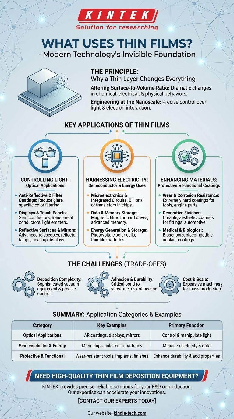
At their core, thin films are used in nearly every piece of modern technology. These microscopically thin layers of material are applied to surfaces to grant them new properties, making them essential for everything from the anti-glare coating on your glasses and the screen of your smartphone to the solar panels that generate clean energy and the protective coatings on industrial tools.
The crucial insight is not just what uses thin films, but why. By reducing a material to a layer often just atoms thick, we fundamentally change how it interacts with light, electricity, and physical stress, unlocking capabilities that are impossible with the material in its bulk form.
The Principle: Why a Thin Layer Changes Everything
Before listing applications, it's essential to understand the principle that makes thin films so powerful. When a material is reduced to a microscopic film, its properties are no longer governed by its internal volume but by its surface.
Altering the Surface-to-Volume Ratio
In a bulk material, the vast majority of atoms are surrounded by other atoms. In a thin film, a significant percentage of atoms are at a surface. This dramatically changes the material's chemical, electrical, and physical behaviors, creating unique properties.
Engineering at the Nanoscale
When a film's thickness is comparable to the wavelength of light or electrons, we gain precise control. We can design layers to selectively reflect or transmit specific colors of light, or to guide the flow of electrons in a way that forms a microscopic circuit.
Controlling Light: Optical Applications
Some of the most common applications of thin films involve the precise manipulation of light. These layers are engineered to bend, reflect, or filter light in highly specific ways.
Anti-Reflective and Filter Coatings
Thin films are applied to eyeglasses, camera lenses, and solar panels to reduce glare and maximize light transmission. Multiple layers can also act as highly specific filters, allowing only a narrow band of colors to pass through, which is critical for optical instruments.
Displays and Touch Panels
Modern LED, LCD, and flexible displays rely on numerous thin film layers. These layers act as semiconductors, transparent conductors, and light-emitting sources that work together to create the images on your screen.
Reflective Surfaces and Mirrors
Beyond simple household mirrors, thin films create specialized reflective surfaces. This includes the mirrors in advanced telescopes, coatings for reflector lamps, and the technology behind head-up displays in modern vehicles.
Harnessing Electricity: Semiconductor and Energy Uses
The entire digital world is built upon thin films that control the flow of electrons. From processing information to generating and storing power, these applications are foundational.
Microelectronics and Integrated Circuits
The microchips at the heart of every computer and smartphone are constructed from dozens of meticulously deposited thin film layers. These layers of semiconductor and insulating materials form the billions of tiny transistors that perform calculations.
Data and Memory Storage
Thin films are fundamental to how we store information. The surfaces of hard drives are coated with magnetic thin films, where data is written and read, while advanced computer memory technologies also rely on thin-film structures.
Energy Generation and Storage
Photovoltaic solar cells convert sunlight into electricity using thin films of semiconductor material. Similarly, the development of thin-film batteries promises lighter, more flexible, and more efficient ways to store energy for everything from wearable devices to electric vehicles.
Enhancing Materials: Protective and Functional Coatings
Thin films are also used to protect surfaces, improve their physical properties, or give them entirely new functions.
Wear and Corrosion Resistance
Extremely hard materials can be deposited as thin films onto industrial cutting tools and engine parts. This provides exceptional wear resistance and protects components from corrosion, significantly extending their operational life.
Decorative Finishes
The durable, shiny coatings on items like bathroom fittings, jewelry, and automotive trim are often thin films. They provide an aesthetic finish while also protecting the underlying material.
Medical and Biological Applications
In the medical field, thin films are used to create biosensors capable of detecting specific molecules. They also serve as specialized coatings on medical implants to ensure they are compatible with the body.
Understanding the Trade-offs
While incredibly versatile, working with thin films presents unique engineering challenges that are important to acknowledge.
Deposition Complexity
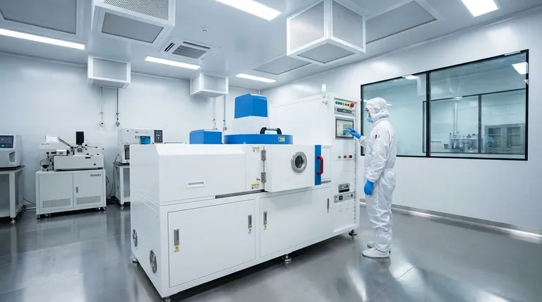
Creating a perfectly uniform, defect-free film that is only a few atoms thick is a highly complex process. It requires sophisticated vacuum equipment and precise control over temperature, pressure, and chemistry.
Adhesion and Durability
A thin film is only as effective as its bond to the underlying material (the substrate). Ensuring strong adhesion is critical, as any peeling or flaking renders the film useless.
Cost and Scale
While the amount of material used in a thin film is minuscule, the machinery and processes required for deposition can be very expensive. Scaling these processes for mass production is a significant industrial challenge.
Identifying Thin Films in Your World
The best way to appreciate the scope of this technology is to recognize its role in the devices and systems you encounter daily.
- If your focus is consumer electronics: See thin films in the anti-glare screen of your laptop, the microchip inside your phone, and the sensors in your smartwatch.
- If your focus is sustainability and energy: Recognize their role in making solar panels more efficient and enabling the development of next-generation batteries.
- If your focus is industrial and automotive: Consider how they provide critical wear resistance on cutting tools and create the reflective surfaces for head-up displays.
Thin films are a foundational, often invisible technology that enhances nearly every aspect of the modern world.
Summary Table:
| Application Category | Key Examples | Primary Function |
|---|---|---|
| Optical Applications | Anti-reflective coatings, displays, mirrors | Control and manipulate light |
| Semiconductor & Energy | Microchips, solar cells, batteries | Manage electricity and data |
| Protective & Functional Coatings | Wear-resistant tools, medical implants, decorative finishes | Enhance durability and add new properties |
Need High-Quality Thin Film Deposition Equipment?
As a leader in advanced lab equipment, KINTEK provides the precise, reliable solutions your R&D or production process demands. Whether you're developing next-generation electronics, durable coatings, or innovative energy systems, our expertise in thin film technology can help you achieve superior results.
Contact our experts today to discuss how KINTEK's specialized equipment can accelerate your thin film innovations.
Visual Guide
Related Products
- Aluminized Ceramic Evaporation Boat for Thin Film Deposition
- Tungsten Evaporation Boat for Thin Film Deposition
- Electron Beam Evaporation Coating Oxygen-Free Copper Crucible and Evaporation Boat
- Molybdenum Tungsten Tantalum Evaporation Boat for High Temperature Applications
- Aluminum-Plastic Flexible Packaging Film for Lithium Battery Packaging
People Also Ask
- What are thin films deposited by evaporation? A Guide to High-Purity Coating
- What is the chemical method for thin film deposition? Build Films from the Molecular Level Up
- Why is an alumina boat selected for catalyst precursors? Ensure Sample Purity at 1000 °C
- Why is an alumina boat and Ti3AlC2 powder bed necessary for Ti2AlC sintering? Protect MAX Phase Purity
- What is the source of evaporation for thin film? Choosing Between Thermal and E-Beam Methods


