In short, gold sputtering is used to apply an ultra-thin, electrically conductive layer of gold onto a non-conductive sample before it is viewed in a Scanning Electron Microscope (SEM). This coating is essential because it prevents the buildup of electrical charge on the sample's surface from the SEM's electron beam, which would otherwise create a distorted and unusable image.
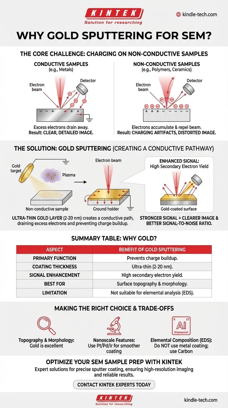
The core challenge of SEM analysis is that the electron beam used to create an image requires the sample to be conductive. Gold sputtering is a standard preparation technique that solves this problem for non-conductive materials, enabling clear, high-resolution imaging of an otherwise invisible microscopic world.
The Fundamental Problem: Electrons and Insulators
To understand why sputtering is necessary, you first have to understand the core mechanics of how an SEM works and the problem that arises with certain materials.
How an SEM Creates an Image
An SEM doesn't see a sample directly. Instead, it scans a focused beam of high-energy electrons across the specimen's surface.
As these primary electrons strike the surface, they knock loose other, lower-energy electrons from the sample itself. These are called secondary electrons.
A detector within the microscope collects these secondary electrons. The number of electrons collected from each point on the surface is used to build a detailed, high-magnification image of the sample's topography (its surface features).
The "Charging" Effect on Non-Conductive Samples
This process works perfectly on conductive materials, like metals, because any excess electrons from the beam are immediately conducted away to the grounded instrument.
However, on a non-conductive or poorly conductive sample (like a ceramic, polymer, or biological specimen), the electrons have nowhere to go. They accumulate on the surface.
This buildup of negative charge, known as specimen charging, repels the incoming electron beam. This interference severely degrades the image, causing bright patches, streaks, and a complete loss of detail.
How Gold Sputtering Solves the Imaging Problem
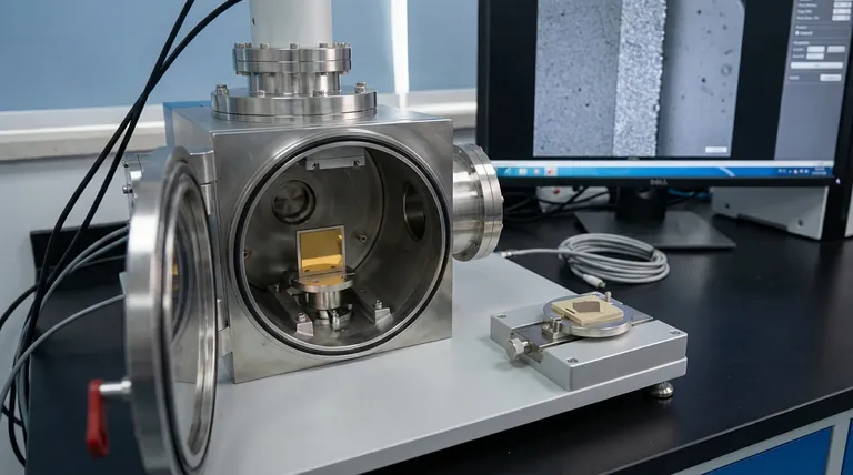
Sputter coating is the solution to this charging effect. The process deposits a metallic film, just a few nanometers thick, that fundamentally changes how the sample interacts with the electron beam.
Creating a Conductive Pathway
The primary function of the gold layer (typically 2-20 nm thick) is to create a conductive path. It covers the entire surface of the insulating specimen and connects it to the grounded metal sample holder.
This path allows the excess electrons from the beam to drain away harmlessly, completely preventing charge buildup.
Enhancing the Imaging Signal
Beyond just preventing charging, gold offers another significant benefit. It has a very high secondary electron yield, meaning it's highly efficient at releasing secondary electrons when struck by the primary beam.
This results in a much stronger, clearer signal for the detector to capture. The outcome is a final image with a significantly improved signal-to-noise ratio, revealing fine surface details that would otherwise be lost.
Understanding the Trade-offs
While gold sputtering is a standard and effective technique, it's a preparatory step with specific consequences that must be considered.
Why Gold is So Common
Gold is a popular choice because it is relatively inert (it won't react with the sample), is very easy to sputter, and provides the excellent secondary electron yield mentioned earlier. For general-purpose imaging of surface morphology, it is the go-to material.
When to Use Other Metals
For extremely high-magnification work, the granular structure of the gold coating itself can become visible. In these cases, metals with a finer grain structure, such as platinum, palladium, or iridium, are often used to produce a smoother, more uniform coating.
The Critical Limitation: Obscuring True Composition
The most significant trade-off is that the coating covers the sample's original surface. This makes sputter coating unsuitable if your goal is elemental analysis (e.g., using Energy-Dispersive X-ray Spectroscopy, or EDS). The gold coating will interfere with or completely block the signals from the actual specimen underneath.
Making the Right Choice for Your Goal
Selecting the right sample preparation is critical for obtaining meaningful data from an SEM.
- If your primary focus is surface topography and morphology: Gold sputtering is an excellent, industry-standard method for imaging non-conductive samples.
- If you need to resolve extremely fine nanoscale features: Consider a finer-grained metal like platinum/palladium or iridium to minimize coating artifacts.
- If your primary focus is elemental composition (EDS): Do not use a metallic sputter coating. The sample must either be analyzed uncoated or prepared with a conductive carbon coating, which produces less interference.
Ultimately, gold sputtering is a foundational technique that makes the vast world of non-conductive materials accessible to the powerful magnification of the SEM.
Summary Table:
| Aspect | Benefit of Gold Sputtering |
|---|---|
| Primary Function | Prevents charge buildup on non-conductive samples |
| Coating Thickness | Ultra-thin layer (2-20 nm) |
| Signal Enhancement | High secondary electron yield for clearer images |
| Best For | Surface topography and morphology analysis |
| Limitation | Not suitable for elemental analysis (EDS) |
Need to optimize your SEM sample preparation? KINTEK specializes in lab equipment and consumables for precise sputter coating solutions. Our expertise ensures your non-conductive samples are perfectly prepared for high-resolution imaging, helping you avoid charging artifacts and achieve reliable results. Contact our experts today to discuss the best coating solution for your specific application!
Visual Guide
Related Products
- RF PECVD System Radio Frequency Plasma-Enhanced Chemical Vapor Deposition RF PECVD
- Inclined Rotary Plasma Enhanced Chemical Vapor Deposition PECVD Equipment Tube Furnace Machine
- Electron Beam Evaporation Coating Oxygen-Free Copper Crucible and Evaporation Boat
- Chemical Vapor Deposition CVD Equipment System Chamber Slide PECVD Tube Furnace with Liquid Gasifier PECVD Machine
- Microwave Plasma Chemical Vapor Deposition MPCVD Machine System Reactor for Lab and Diamond Growth
People Also Ask
- What are the applications of PECVD? Essential for Semiconductors, MEMS, and Solar Cells
- Why is PECVD environment friendly? Understanding the Eco-Friendly Benefits of Plasma-Enhanced Coating
- How are PECVD and CVD different? A Guide to Choosing the Right Thin-Film Deposition Process
- What is the principle of plasma enhanced chemical vapor deposition? Achieve Low-Temperature Thin Film Deposition
- How does RF power create plasma? Achieve Stable, High-Density Plasma for Your Applications