Plasma-Enhanced Chemical Vapor Deposition (PECVD) is the essential method for silicon nitride (SiNy) deposition because it utilizes high-frequency plasma to drive chemical reactions at significantly lower temperatures than traditional thermal processes. This low-temperature environment—typically between 200°C and 400°C—is critical for maintaining the structural integrity of underlying sensitive layers, such as ultra-thin silicon oxide (SiOx), while ensuring the resulting film is dense, uniform, and highly conformal.
Core Takeaway: PECVD is required because it enables the deposition of high-performance passivation films without exceeding the "thermal budget" of the device. It provides a unique combination of low-heat processing and active hydrogen passivation that cannot be achieved through standard furnace-based methods.
Preserving the Thermal Budget
Protecting Underlying Structures
Advanced semiconductor and solar cell architectures often rely on ultra-thin interface layers, such as 8 nm SiOx. Traditional thermal CVD requires extreme heat that would degrade or destroy these delicate structures.
PECVD uses plasma energy rather than thermal energy to excite reaction gases like silane (SiH4) and ammonia (NH3). This allows the substrate to remain at a relatively cool 200°C, preserving the integrity of the layers already deposited on the wafer.
Versatility in Manufacturing
By operating at lower temperatures, PECVD allows manufacturers to integrate silicon nitride into various stages of production where high heat is no longer an option. This is particularly vital for large-scale (LSI) and very-large-scale integrated circuits (VLSI) where multiple layers of different materials are stacked.
Superior Film Quality and Step Coverage
Achieving High Density and Uniformity
Despite the low deposition temperature, PECVD produces SiNy films with low pinhole density and high structural density. These characteristics are vital for creating an effective barrier against moisture and contaminants.
Excellent Step Coverage and Conformality
PECVD is known for its ability to provide good coverage of component edges, also known as step coverage. This ensures that the silicon nitride layer wraps uniformly around complex 3D structures on the wafer, providing consistent protection across the entire surface.
Growth Rate and Productivity
The plasma-enhanced environment enables faster growth rates compared to many other low-temperature techniques. This high throughput makes it an economically viable choice for mass production in the semiconductor and solar industries.
Electronic and Chemical Passivation
Field-Effect and Chemical Passivation
Silicon nitride serves as more than just a physical barrier; it provides field-effect and chemical passivation. This reduces the "surface carrier recombination rate," which is a fancy way of saying it prevents lost energy in solar cells and improves electrical efficiency in circuits.
Bulk Passivation via Hydrogenation
During the PECVD process, hydrogen plasma is generated and incorporated into the film (often denoted as SiNx:H). This hydrogen can later migrate into the silicon wafer to repair internal defects and "dangle bonds."
This bulk passivation effect is a critical secondary benefit of PECVD. It significantly boosts the overall electrical performance of the device by neutralizing flaws within the silicon material itself.
Understanding the Trade-offs
Film Stress and Stoichiometry
While PECVD is highly versatile, the resulting films can vary in internal stress. Depending on the plasma frequency and gas ratios, the film may be stoichiometric, low-pressure, or super-low stress.
Chemical Complexity
Because hydrogen is inherently part of the PECVD process, the films are rarely pure Si3N4. The presence of hydrogen (SiNx:H) is beneficial for passivation but can be a drawback if the application requires a perfectly pure, hydrogen-free dielectric.
How to Apply This to Your Project
Making the Right Choice for Your Goal
- If your primary focus is solar cell efficiency: Use PECVD to take advantage of the hydrogen-rich environment, which provides both surface passivation and internal defect repair (bulk passivation).
- If your primary focus is protecting sensitive thin films: Prioritize PECVD systems that operate at the lowest possible temperature (near 200°C) to avoid damaging underlying SiOx or metal layers.
- If your primary focus is barrier protection in ICs: Focus on PECVD recipes that minimize pinhole density and maximize conformality to ensure the SiNy layer acts as an effective diffusion mask.
By decoupling chemical reactions from substrate temperature, PECVD remains the definitive tool for high-performance silicon nitride deposition in modern electronics.
Summary Table:
| Feature | Benefit | Key Application |
|---|---|---|
| Low Temperature (200-400°C) | Protects delicate underlying layers (e.g., SiOx) | Advanced IC & Solar Cell Fabrication |
| Plasma-Driven Chemistry | High growth rates & throughput | Mass Production (LSI/VLSI) |
| Hydrogen Incorporation | Repairs internal defects (Bulk Passivation) | Enhancing Solar Cell Efficiency |
| High Conformality | Excellent step coverage on 3D structures | Complex Semiconductor Architectures |
| Film Density | Effective barrier against moisture/contaminants | Device Encapsulation & Protection |
Elevate Your Thin-Film Precision with KINTEK
Maximize your device performance and protect your thermal budget with KINTEK’s advanced PECVD and CVD systems. Whether you are developing next-generation solar cells requiring bulk hydrogenation or complex integrated circuits needing superior step coverage, our equipment delivers the density and uniformity your project demands.
Why partner with KINTEK?
- Comprehensive Range: From PECVD and MPCVD systems to high-temperature muffle and vacuum furnaces.
- Specialized Solutions: High-temperature high-pressure reactors, autoclaves, and precision hydraulic presses.
- Expert Support: We provide the tools and consumables—including ceramics, crucibles, and PTFE products—to ensure seamless lab operations.
Ready to optimize your deposition process? Contact our technical experts today to find the perfect solution for your lab!
References
- Caroline Lima Anderson, Sumit Agarwal. Pinhole electrical conductivity in polycrystalline Si on locally etched SiN /SiO passivating contacts for Si solar cells. DOI: 10.1016/j.mssp.2023.107655
This article is also based on technical information from Kintek Solution Knowledge Base .
Related Products
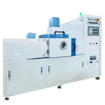
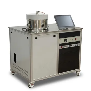
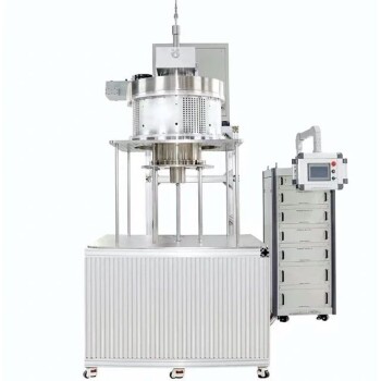
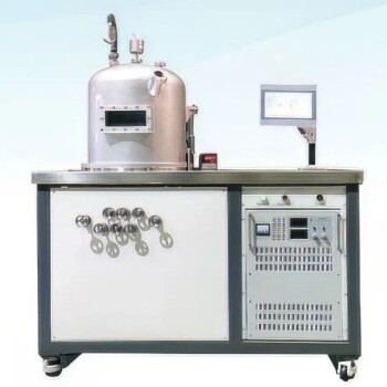
- RF PECVD System Radio Frequency Plasma-Enhanced Chemical Vapor Deposition RF PECVD
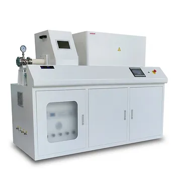
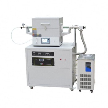
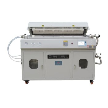
- Chemical Vapor Deposition CVD Equipment System Chamber Slide PECVD Tube Furnace with Liquid Gasifier PECVD Machine
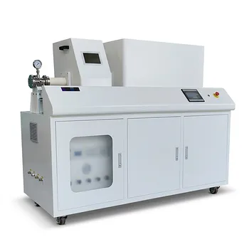
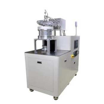
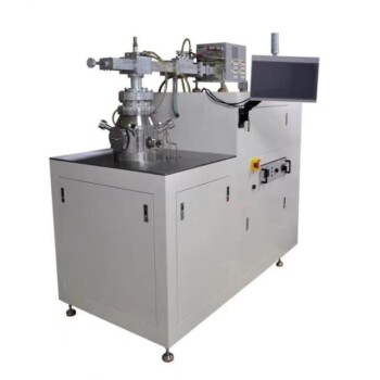
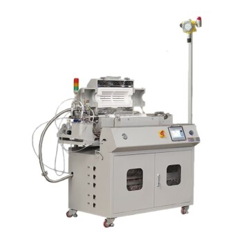
- Inclined Rotary Plasma Enhanced Chemical Vapor Deposition PECVD Equipment Tube Furnace Machine
- Inclined Rotary Plasma Enhanced Chemical Vapor Deposition PECVD Equipment Tube Furnace Machine
- 915MHz MPCVD Diamond Machine Microwave Plasma Chemical Vapor Deposition System Reactor
People Also Ask
- What is plasma enhanced chemical vapour deposition PECVD used for? Enable Low-Temp Thin Films for Electronics & Solar
- What is an example of PECVD? RF-PECVD for High-Quality Thin Film Deposition
- What is the role of RF-PECVD in VFG preparation? Mastering Vertical Growth and Surface Functionality
- What is plasma enhanced chemical Vapour deposition process used for fabrication of? A Guide to Low-Temperature Thin Films
- What is plasma chemical vapor deposition? A Low-Temperature Thin Film Coating Solution