In short, Plasma-Enhanced Chemical Vapor Deposition (PECVD) is a cornerstone process used to fabricate high-quality thin films. Its applications are central to modern technology, including the manufacturing of microchips, solar panels, and specialized optical and protective coatings.
The core value of PECVD is its ability to deposit durable, uniform thin films at significantly lower temperatures than traditional methods. This capability is not just an improvement; it is the enabling technology that allows for the creation of complex, multi-layered electronic devices on temperature-sensitive materials.
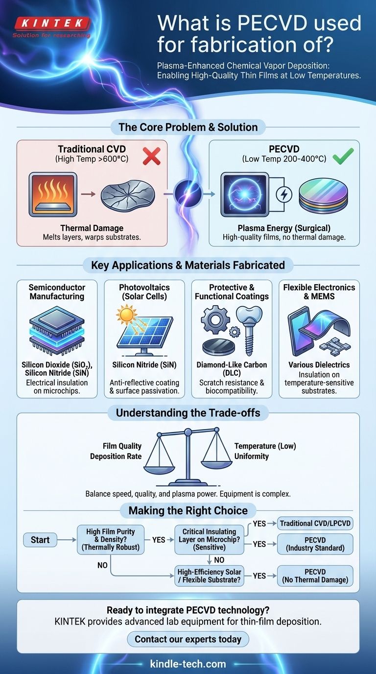
The Core Problem PECVD Solves: High-Temperature Damage
To understand why PECVD is so critical, one must first understand the limitations of its predecessor, conventional Chemical Vapor Deposition (CVD).
The Challenge with Traditional CVD
Traditional CVD processes rely on very high temperatures (often >600°C) to provide the energy needed for chemical reactions to occur, forming a solid film from a gas precursor.
This extreme heat is a major problem when building modern electronics. It can melt previously deposited metal layers, damage delicate transistors, or warp the underlying substrate, destroying the device.
How PECVD Breaks the Temperature Barrier
PECVD circumvents this problem by using a different energy source: plasma.
Instead of heating the entire chamber, an electric field is applied to the precursor gas, ionizing it and creating a glowing, highly energetic state of matter known as plasma.
This plasma provides the necessary energy to drive the chemical reactions at the substrate surface, allowing for high-quality film deposition at much lower temperatures, typically in the 200-400°C range.
Key Applications and Materials Fabricated
The low-temperature advantage makes PECVD indispensable across several high-tech industries.
Semiconductor Manufacturing
This is the primary application of PECVD. It is used to deposit dielectric (insulating) films like silicon dioxide (SiO₂) and silicon nitride (SiN) on silicon wafers.
These films are essential for insulating the microscopic metal wires that connect millions of transistors on a single chip. Without the low-temperature capability of PECVD, manufacturing these complex, multi-layered integrated circuits would be impossible.
Photovoltaics (Solar Cells)
PECVD is critical for improving the efficiency of solar cells. It is used to deposit two key layers.
First, a silicon nitride anti-reflective coating is applied to the surface, which minimizes light reflection and allows more photons to enter the cell. Second, it's used for surface passivation layers that reduce energy losses, boosting overall device performance.
Protective and Functional Coatings
The process is used to create hard, durable coatings on a variety of materials.
For example, diamond-like carbon (DLC) films can be deposited on machine tools for scratch resistance or on medical implants for biocompatibility. These films are valued for their hardness and low friction.
Flexible Electronics and MEMS
The ability to deposit films on temperature-sensitive polymers makes PECVD essential for the growing field of flexible electronics.
It is also used in the fabrication of Micro-Electro-Mechanical Systems (MEMS), where complex, delicate structures cannot withstand high processing temperatures.
Understanding the Trade-offs
While powerful, PECVD is not a universal solution. It involves specific trade-offs that are important to recognize.
Film Quality vs. Temperature
PECVD films are high-quality, but they can contain more hydrogen and have a slightly lower density than films grown at very high temperatures via conventional CVD. This is a direct trade-off for the benefit of a low-temperature process.
Deposition Rate vs. Uniformity
Engineers must balance deposition speed with film quality. Increasing the plasma power can speed up the process, but it can sometimes lead to non-uniformity across the substrate and may introduce stress into the film.
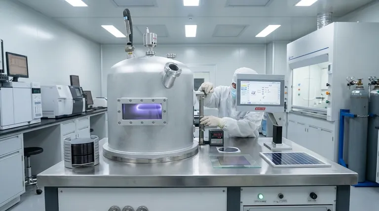
Equipment Complexity
PECVD reactors are more complex and expensive than many other deposition systems. They require sophisticated vacuum chambers, gas handling systems, and radio-frequency (RF) or microwave power sources to generate and sustain the plasma.
Making the Right Choice for Your Goal
Selecting a deposition method depends entirely on the requirements of the final device and the limitations of your substrate.
- If your primary focus is the absolute highest film purity and density on a thermally robust substrate: A high-temperature process like traditional CVD or LPCVD may be the superior choice.
- If your primary focus is depositing a critical insulating layer onto a completed microchip with sensitive transistors: PECVD is the non-negotiable industry standard.
- If your primary focus is creating high-efficiency solar cells or coating a flexible plastic substrate: PECVD provides the necessary film properties without causing thermal damage.
Ultimately, PECVD's genius lies in its ability to use energy surgically, building the microscopic world of modern electronics without destroying it in the process.
Summary Table:
| Key Application | Material Fabricated | Primary Function |
|---|---|---|
| Semiconductor Manufacturing | Silicon Dioxide (SiO₂), Silicon Nitride (SiN) | Electrical insulation on microchips |
| Photovoltaics (Solar Cells) | Silicon Nitride (SiN) | Anti-reflective coating & surface passivation |
| Protective Coatings | Diamond-Like Carbon (DLC) | Scratch resistance & biocompatibility |
| Flexible Electronics/MEMS | Various Dielectrics | Insulation on temperature-sensitive substrates |
Ready to integrate PECVD technology into your fabrication process?
KINTEK specializes in providing advanced lab equipment and consumables for thin-film deposition and materials science. Whether you are developing the next generation of microchips, high-efficiency solar cells, or specialized coatings, our expertise can help you achieve superior film quality and process efficiency.
Contact our experts today to discuss how our solutions can meet your specific laboratory needs and drive your innovations forward.
Visual Guide
Related Products
- RF PECVD System Radio Frequency Plasma-Enhanced Chemical Vapor Deposition RF PECVD
- Chemical Vapor Deposition CVD Equipment System Chamber Slide PECVD Tube Furnace with Liquid Gasifier PECVD Machine
- Inclined Rotary Plasma Enhanced Chemical Vapor Deposition PECVD Equipment Tube Furnace Machine
- Inclined Rotary Plasma Enhanced Chemical Vapor Deposition PECVD Equipment Tube Furnace Machine
- Microwave Plasma Chemical Vapor Deposition MPCVD Machine System Reactor for Lab and Diamond Growth
People Also Ask
- What is the role of RF-PECVD in VFG preparation? Mastering Vertical Growth and Surface Functionality
- How does plasma enhance CVD? Unlock Low-Temperature, High-Quality Film Deposition
- What is plasma CVD? Unlock Low-Temperature Thin Film Deposition for Sensitive Materials
- What is an example of PECVD? RF-PECVD for High-Quality Thin Film Deposition
- What is plasma enhanced chemical vapour deposition PECVD used for? Enable Low-Temp Thin Films for Electronics & Solar


