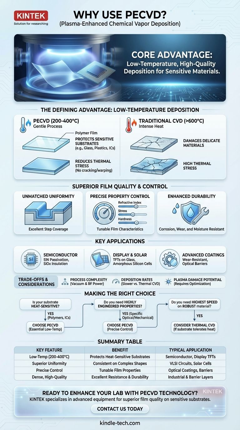
The core advantage of PECVD is simple: it allows for the deposition of high-quality, uniform thin films at significantly lower temperatures than traditional methods. This capability is critical for coating temperature-sensitive materials, such as those used in modern electronics and polymers, without causing damage or thermal stress.
PECVD is not just a low-temperature alternative; it's a strategic choice for applications demanding high-performance protective or functional layers on substrates that cannot withstand heat. Its value lies in the unique combination of gentle processing with precise control over the final film's properties.
The Defining Advantage: Low-Temperature Deposition
The most significant reason to use Plasma-Enhanced Chemical Vapor Deposition (PECVD) is its ability to operate at low temperatures, often between 200°C and 400°C. This fundamentally expands the range of materials and devices that can be coated.
Protecting Sensitive Substrates
Traditional Chemical Vapor Deposition (CVD) often requires temperatures exceeding 600°C, which can damage or destroy delicate substrates.
PECVD uses plasma to supply the energy needed to activate precursor gases, replacing the need for intense heat. This makes it ideal for coating materials like glass, plastics, and fully assembled integrated circuits.
Reducing Thermal Stress
By avoiding high temperatures, PECVD minimizes the thermal stress that can cause thin films to crack, delaminate, or warp. This results in a more reliable and durable final product.
Achieving Superior Film Quality and Control
Beyond its low-temperature operation, PECVD provides an exceptional degree of control over the final film, leading to higher-quality and more functional coatings.
Unmatched Uniformity and Coverage
The plasma-assisted process enables highly uniform film deposition across the entire surface of a substrate, even on complex shapes. This ensures consistent performance and is often referred to as good "step coverage."
Precise Control Over Material Properties
Engineers can precisely tune the final film's characteristics by adjusting process parameters. This includes properties like refractive index, material stress, hardness, and chemical composition.
Enhanced Durability and Protection
The resulting films are dense and high-quality, providing excellent protective barriers. PECVD coatings are widely used for their corrosion-resistant, waterproof, anti-aging, and wear-resistant properties.
Key Applications in Modern Technology
PECVD's unique combination of low temperature and high control has made it an indispensable process in several high-tech industries.
Semiconductor Manufacturing
In the production of Very Large-Scale Integrated (VLSI) circuits, PECVD is used to deposit silicon nitride (SiN) films as a final protective layer and silicon oxide (SiOx) as an insulating layer between metal tracks.
Display and Solar Technology
The technology is critical for manufacturing thin-film transistors (TFTs) used in active-matrix LCD displays, as it allows for deposition on large glass substrates without damage. It is also used in the fabrication of amorphous silicon solar cells.
Advanced Protective Coatings
PECVD is used to create specialized coatings like wear-resistant titanium carbide (TiC) films and aluminum oxide barrier films for a variety of industrial and consumer products.
Understanding the Trade-offs and Considerations
While powerful, PECVD is not a universal solution. An objective assessment requires understanding its potential downsides compared to other methods.
Process Complexity
PECVD systems require sophisticated vacuum chambers and radio-frequency (RF) power sources to generate and sustain the plasma. This equipment can be more complex and costly than traditional thermal CVD furnaces.
Deposition Rates
While highly controllable, the deposition rates for PECVD can sometimes be lower than those of high-temperature thermal CVD processes. This is a classic trade-off between manufacturing speed and film quality on sensitive substrates.
Potential for Plasma Damage
The high-energy ions within the plasma can, if not properly controlled, cause damage to the substrate surface. Optimizing the process is critical to mitigate this risk, especially in sensitive electronic applications.
Making the Right Choice for Your Application
Selecting the right deposition method depends entirely on your material, substrate, and performance goals.
- If your primary focus is coating heat-sensitive materials (like polymers or integrated circuits): PECVD is almost always the superior choice due to its essential low-temperature process.
- If your primary focus is creating highly engineered films with specific optical or mechanical properties: PECVD offers the precise control over composition, stress, and uniformity required for these advanced applications.
- If your primary focus is achieving the highest deposition speed for a simple, robust material: You should evaluate whether a traditional high-temperature CVD process might be a more cost-effective alternative, provided your substrate can tolerate the heat.
Ultimately, leveraging PECVD allows you to engineer advanced material properties onto surfaces that were previously off-limits to high-performance coatings.
Summary Table:
| Key Feature | Benefit | Typical Application |
|---|---|---|
| Low-Temperature Operation (200-400°C) | Protects heat-sensitive substrates (polymers, ICs) | Semiconductor passivation, display TFTs |
| Superior Film Uniformity & Step Coverage | Consistent performance on complex shapes | VLSI circuits, solar cells |
| Precise Control of Film Properties | Tunable refractive index, stress, hardness | Optical coatings, protective barriers |
| Dense, High-Quality Films | Excellent corrosion, wear, and moisture resistance | Industrial coatings, barrier layers |
Ready to enhance your lab's capabilities with PECVD technology?
KINTEK specializes in advanced lab equipment and consumables for precise thin-film deposition. Our solutions help you achieve superior film quality on sensitive substrates—ensuring reliability and performance for your semiconductor, display, or coating applications.
Contact us today to discuss how PECVD can solve your specific material challenges!
Visual Guide
Related Products
- Inclined Rotary Plasma Enhanced Chemical Vapor Deposition PECVD Equipment Tube Furnace Machine
- Chemical Vapor Deposition CVD Equipment System Chamber Slide PECVD Tube Furnace with Liquid Gasifier PECVD Machine
- Inclined Rotary Plasma Enhanced Chemical Vapor Deposition PECVD Equipment Tube Furnace Machine
- RF PECVD System Radio Frequency Plasma-Enhanced Chemical Vapor Deposition RF PECVD
- Multi Heating Zones CVD Tube Furnace Machine Chemical Vapor Deposition Chamber System Equipment
People Also Ask
- How does PECVD facilitate Ru-C nanocomposite films? Precision Low-Temperature Thin Film Synthesis
- What are the benefits of plasma enhanced CVD? Achieve High-Quality, Low-Temperature Film Deposition
- How does PECVD equipment facilitate the directional growth of carbon nanotubes? Achieve Precision Vertical Alignment
- What is plasma enhanced chemical vapour deposition PECVD used for? Enable Low-Temp Thin Films for Electronics & Solar
- What is plasma enhanced chemical vapor deposition PECVD equipment? A Guide to Low-Temperature Thin Film Deposition


