Fundamentals of the Annealing Process
Lattice Damage Repair
The annealing process plays a pivotal role in repairing lattice damage induced by ion implantation. This critical step involves subjecting the semiconductor material to high-temperature treatment, which facilitates the restoration of the crystalline lattice's order. The high temperatures cause the displaced atoms to reorient themselves, effectively healing the structural imperfections created during the implantation process.
To achieve optimal results, the annealing temperature must be precisely controlled. Typically, temperatures ranging from 500°C to 950°C are employed, depending on the specific type of lattice damage and the desired outcome. For instance, lower temperatures are often sufficient for minor lattice disruptions, while higher temperatures are necessary for more severe damage.
| Temperature Range | Purpose |
|---|---|
| 500°C - 600°C | Minor lattice repair |
| 700°C - 800°C | Moderate lattice repair |
| 900°C - 950°C | Severe lattice repair and impurity activation |
The duration of the annealing process is equally important. Prolonged exposure to high temperatures can lead to unwanted diffusion of impurities, whereas shorter durations may not provide sufficient time for the lattice to fully recover. Therefore, a careful balance between temperature and time is essential to ensure both effective lattice repair and minimal collateral damage.
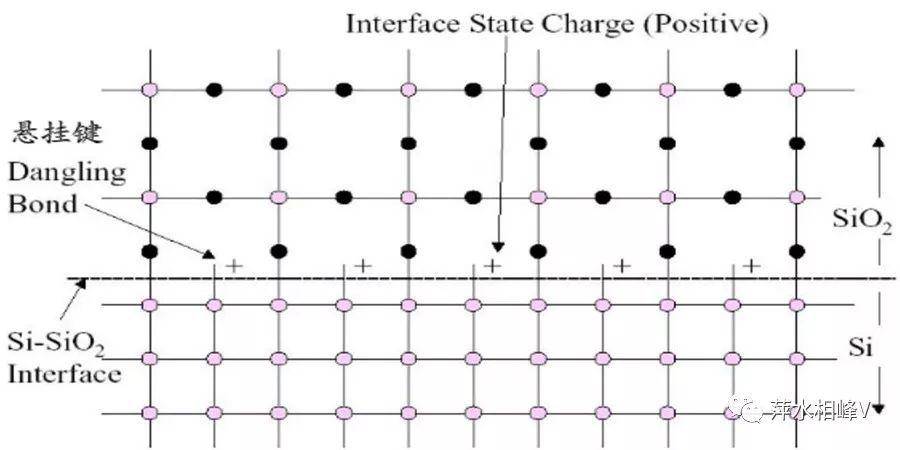
In summary, the annealing process is indispensable for restoring the structural integrity of semiconductor materials post-implantation. By meticulously controlling the temperature and duration of the treatment, manufacturers can achieve the desired lattice order, thereby enhancing the overall performance and reliability of semiconductor devices.
Impurity Activation
Annealing plays a pivotal role in activating dopants by facilitating the migration of impurity atoms to lattice sites. This process typically necessitates temperatures around 950°C, which creates an environment conducive to the atomic rearrangements necessary for dopant activation.
During annealing, the high temperature induces thermal energy that overcomes the binding energy of the impurity atoms, allowing them to diffuse and occupy lattice positions. This movement is crucial for establishing the desired electrical properties in the semiconductor material. The activation of dopants is essential for controlling the conductivity and performance of semiconductor devices, making it a critical step in the fabrication process.
Moreover, the precise control of temperature during annealing is vital. Temperatures that are too low may result in insufficient dopant activation, while temperatures that are too high could lead to excessive diffusion, altering the intended doping profile. Therefore, maintaining the optimal temperature range is key to achieving the desired electrical characteristics and ensuring the reliability of semiconductor devices.
Film Modification
Annealing plays a pivotal role in refining the structural integrity of semiconductor films, particularly those utilized in high-k gate dielectrics. This process involves subjecting the films to controlled high-temperature treatments, which induces a series of physical and chemical transformations.
Firstly, annealing densifies the initially loose and porous film structure. This densification process reduces the film's porosity, leading to a more uniform and compact lattice. The reduction in voids and defects enhances the overall mechanical stability of the film, making it less susceptible to cracking and delamination during subsequent fabrication steps.
Secondly, the thermal treatment during annealing significantly improves the electrical properties of high-k gate dielectrics. High-k materials, such as hafnium oxide (HfO₂) and zirconium oxide (ZrO₂), are critical for reducing leakage currents and improving capacitance in modern transistors. Annealing optimizes the dielectric constant and reduces interface trap density, thereby enhancing the film's ability to store charge and maintain high-speed switching in transistors.
Moreover, the improved film properties directly contribute to enhanced device performance. By ensuring that the high-k gate dielectrics are of high quality, the annealing process helps in achieving better transistor characteristics, including lower power consumption, higher switching speeds, and improved reliability. This is particularly important as semiconductor manufacturers continue to push the boundaries of device miniaturization and performance optimization.
In summary, annealing's impact on film modification is multifaceted, encompassing densification, electrical property enhancement, and overall device performance improvement. These benefits underscore the critical role of annealing in the sophisticated landscape of semiconductor fabrication.
Metal Silicide Formation
The formation of metal silicides during the annealing process plays a pivotal role in optimizing both contact and body resistance, which are critical for enhancing the overall performance of semiconductor devices. This crucial step involves the controlled interaction of metal layers with silicon substrates, leading to the formation of stable and low-resistance silicide phases.
The temperature and time parameters during annealing are meticulously managed to ensure the desired phase transformation. Typically, temperatures range from 300°C to 600°C, depending on the specific metal and silicon combination. For instance, nickel silicide (NiSi) formation often requires temperatures around 400°C, while cobalt silicide (CoSi2) may necessitate higher temperatures up to 600°C. The duration of annealing can vary from a few seconds to several minutes, depending on the thermal budget and the specific requirements of the semiconductor device.
| Metal | Silicide Phase | Annealing Temperature (°C) | Annealing Time |
|---|---|---|---|
| Nickel | NiSi | 400 | 1-5 minutes |
| Cobalt | CoSi2 | 600 | 1-3 minutes |
| Titanium | TiSi2 | 650 | 1-2 minutes |
Controlling these parameters is essential to prevent undesired reactions and to ensure the formation of the correct silicide phase. Rapid thermal annealing (RTA) and flash lamp annealing (FLA) are often employed to achieve precise temperature control and rapid heating and cooling cycles, which are particularly beneficial for forming ultra-shallow junctions and advanced node manufacturing.
The benefits of metal silicide formation extend beyond just reducing resistance. The formation of silicides also improves the thermal stability of the contacts, reduces contact resistivity, and enhances the overall reliability of the semiconductor device. This makes it a vital step in the fabrication of high-performance integrated circuits, particularly for advanced nodes and 3D integration technologies.

Key Parameters in Annealing
Temperature
Temperature is a pivotal parameter in the annealing process, significantly influencing the outcome of various stages in semiconductor fabrication. The temperature range during annealing can vary widely, from as low as 500°C for repairing lattice damage to as high as 950°C for activating impurities.
-
Lattice Damage Repair: At temperatures around 500°C, the annealing process primarily focuses on restoring the crystalline structure of the semiconductor material. This is crucial after ion implantation, which often results in lattice disruption. The high-temperature treatment helps in reordering the lattice, ensuring the material's structural integrity is preserved.
-
Impurity Activation: Elevating the temperature to approximately 950°C is necessary for the activation of dopants. At this temperature, impurity atoms can migrate to their designated lattice sites, enabling the desired electrical properties to be achieved. This high-temperature step is essential for ensuring that the dopants are effectively integrated into the semiconductor lattice.
-
Film Modification: Intermediate temperatures are also used to modify the properties of thin films, such as high-k gate dielectrics. By carefully controlling the temperature, the annealing process can densify loose films and enhance their dielectric properties, which is critical for improving device performance.
The precise control of temperature during annealing is therefore not just a technical requirement but a strategic element that directly impacts the quality and functionality of the final semiconductor product.
Time
Annealing time is a critical parameter that must be meticulously balanced with temperature to achieve the desired outcomes in semiconductor fabrication. This balance is essential to prevent the excessive diffusion of impurities, which can lead to unwanted electrical characteristics in the final device. For instance, if the annealing time is too long, impurities may spread beyond their intended regions, causing unintended conductivity paths or reducing the effectiveness of the doping process.
Conversely, an insufficient annealing time may fail to activate the dopants fully or repair lattice damage adequately. This could result in suboptimal device performance, as the semiconductor material would not exhibit the desired electrical properties. Therefore, the duration of the annealing process must be precisely controlled, often ranging from a few seconds in rapid thermal annealing (RTA) to several hours in high-temperature furnace annealing, depending on the specific requirements of the fabrication process.
The optimal annealing time is influenced by several factors, including the type of dopant used, the initial concentration of impurities, and the specific properties of the semiconductor material. For example, in the formation of ultra-shallow junctions, where the depth of the junction is critical, very short annealing times are employed to minimize diffusion while ensuring high activation rates. This is particularly relevant in advanced nodes, where the linewidths are below 20nm and the margin for error is exceedingly narrow.
In summary, the careful management of annealing time is pivotal in semiconductor manufacturing, ensuring that the material properties are precisely tailored to meet the stringent requirements of modern electronic devices.
Thermal Budget
As semiconductor technology advances and nodes shrink, the cumulative thermal impact becomes increasingly critical. This cumulative heat, often referred to as the thermal budget, is the total amount of thermal energy applied during the fabrication process. Minimizing this budget is essential to prevent unwanted diffusion of impurities, maintain device integrity, and ensure optimal performance.
To achieve this, optimized annealing processes are required. These processes must balance the need for high temperatures to activate dopants and repair lattice damage with the necessity of rapid cooling to limit thermal diffusion. Techniques such as Rapid Thermal Annealing (RTA) and Flash Lamp Annealing (FLA) have emerged as key solutions. RTA, for instance, uses rapid heating and cooling cycles to complete the annealing process in seconds, minimizing the time impurities are exposed to high temperatures. Similarly, FLA employs high-intensity flash lamps to achieve rapid annealing in milliseconds, making it ideal for ultra-shallow doping activation with linewidths below 20nm.
The importance of managing the thermal budget is underscored by its direct impact on device performance and reliability. Excessive thermal energy can lead to impurity diffusion, defect formation, and structural degradation, all of which can compromise the integrity of advanced semiconductor devices. Therefore, as technology nodes continue to shrink, the development and implementation of more precise and efficient annealing techniques will be paramount.
Types of Annealing Processes
High-Temperature Furnace Annealing
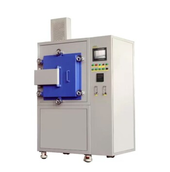
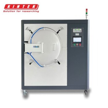
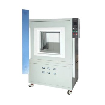
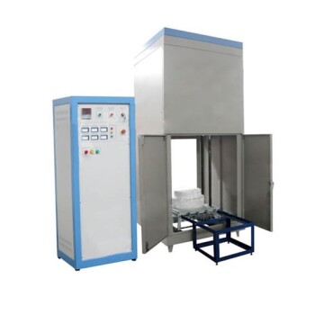
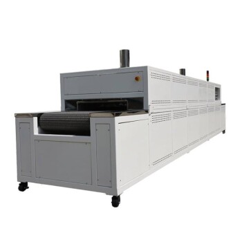
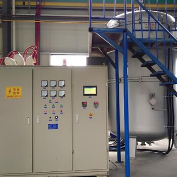
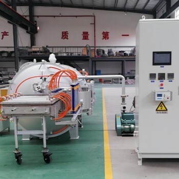
High-temperature furnace annealing is a traditional method that employs elevated temperatures and extended durations, making it ideal for applications with a high thermal budget, such as the preparation of Silicon-on-Insulator (SOI) substrates. This method leverages the fundamental principles of annealing to alter the mechanical properties of materials, enhancing their ductility and reducing their hardness.
The process involves three primary stages:
- Recovery: The furnace initially heats the material to relieve internal stresses, which are often residual from previous manufacturing steps.
- Recrystallization: The material is then heated above its recrystallization temperature but below its melting point. This stage is critical as it facilitates the formation of new grains, which are essential for modifying the material's properties.
- Grain Growth: As the material cools, the newly formed grains grow, further enhancing the material's pliability and overall structural integrity.
A controlled furnace atmosphere is paramount to the success of this process. Without it, the high temperatures involved could lead to surface oxidation and undesirable decarburization, compromising the material's quality. This controlled environment is particularly crucial for annealing stainless steels and non-ferrous metals, ensuring consistent and reproducible results.
In the context of semiconductor manufacturing, high-temperature furnace annealing plays a vital role in preparing substrates that require robust mechanical and electrical properties. The extended heating times and high temperatures ensure that the material undergoes thorough transformation, making it suitable for subsequent fabrication steps that demand high precision and reliability.
Rapid Thermal Annealing (RTA)
Rapid Thermal Annealing (RTA) revolutionizes the semiconductor manufacturing process by employing rapid heating and cooling cycles to achieve annealing in mere seconds. This technique is particularly advantageous for forming ultra-shallow junctions and facilitating advanced node manufacturing. RTA's rapid thermal cycles minimize the diffusion of impurities, ensuring that dopants remain localized and highly activated, which is critical for maintaining performance in ever-shrinking technology nodes.
The speed of RTA allows for precise control over the thermal budget, a key parameter in modern semiconductor fabrication. By limiting the time at elevated temperatures, RTA prevents unwanted thermal diffusion, which can degrade device performance. This makes RTA an ideal choice for processes requiring ultra-shallow junctions, where maintaining the integrity of the junction profile is paramount.
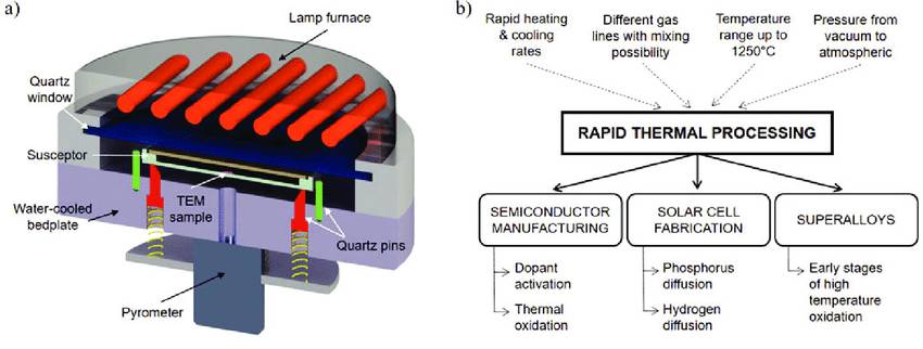
Moreover, RTA's ability to rapidly heat and cool substrates enables the formation of high-quality, ultra-shallow junctions with minimal thermal damage. This is particularly beneficial in advanced node manufacturing, where the demands for precise control and high-quality junctions are more stringent than ever. The rapid thermal cycles of RTA also contribute to the formation of metal silicides, further enhancing device performance by optimizing contact and body resistance.
In summary, RTA's rapid thermal processing capabilities make it an indispensable tool in the arsenal of modern semiconductor manufacturing, particularly for applications requiring ultra-shallow junctions and advanced node fabrication.
Flash Lamp Annealing (FLA)
Flash Lamp Annealing (FLA) represents a cutting-edge technique in semiconductor manufacturing, leveraging high-intensity flash lamps to achieve rapid annealing within milliseconds. This method is particularly advantageous for the activation of ultra-shallow dopants, making it ideal for processes requiring linewidths below 20nm.
Key Features of FLA
- Ultra-Fast Annealing: FLA's rapid thermal treatment significantly reduces the annealing time compared to traditional methods, minimizing thermal budget and preventing excessive diffusion of dopants.
- Precision and Control: The high-intensity flash lamps provide precise control over the annealing process, ensuring uniform heating and optimal activation of dopants.
- Compatibility with Advanced Nodes: FLA's ability to handle ultra-shallow junctions aligns perfectly with the demands of advanced semiconductor nodes, such as FinFET and high-k/metal gate devices.
Comparison with Other Annealing Techniques
| Technique | Heating Method | Annealing Time | Suitability |
|---|---|---|---|
| High-Temperature Furnace Annealing | Conventional heating | Minutes to hours | High thermal budget applications |
| Rapid Thermal Annealing (RTA) | Rapid heating and cooling | Seconds | Ultra-shallow junctions, advanced nodes |
| Flash Lamp Annealing (FLA) | High-intensity flash lamps | Milliseconds | Ultra-shallow doping activation, linewidths < 20nm |
| Laser Spike Annealing (LSA) | Laser light | Milliseconds | Localized, high-precision annealing |
FLA's unique capabilities make it a pivotal technology in the ongoing evolution of semiconductor fabrication, particularly as the industry continues to push the boundaries of device miniaturization and performance.
Laser Spike Annealing (LSA)
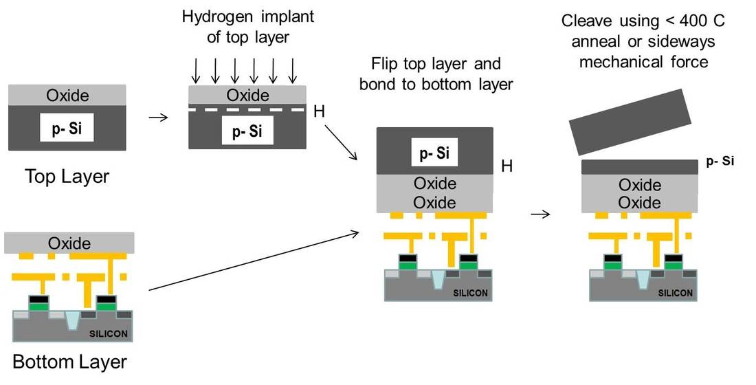
Laser Spike Annealing (LSA) represents a cutting-edge technique in semiconductor fabrication, leveraging the power of laser light to achieve localized, high-precision annealing. This method is particularly advantageous for advanced nodes such as FinFETs and high-k/metal gate devices, where the need for precise control over dopant activation and lattice damage repair is paramount.
Unlike traditional thermal annealing methods that require higher temperatures and longer durations, LSA operates by focusing a high-intensity laser pulse onto specific areas of the semiconductor material. This localized heating allows for the rapid melting and subsequent rapid solidification of the material, enabling the activation of dopants with minimal diffusion. The process typically occurs in nanoseconds, making it an ideal choice for ultra-shallow junction formation and the modification of high-k gate dielectrics.
The benefits of LSA are manifold:
- Precision: The localized nature of laser annealing ensures that only the targeted areas are affected, reducing the risk of thermal damage to surrounding regions.
- Speed: LSA can complete the annealing process in nanoseconds, significantly faster than conventional methods, which is crucial for maintaining high activation rates in shrinking technology nodes.
- Minimized Thermal Budget: By focusing on specific areas, LSA minimizes the overall thermal impact, making it suitable for advanced nodes where thermal budget constraints are critical.
In the context of modern semiconductor manufacturing, LSA's ability to deliver high precision and speed makes it an indispensable tool for enhancing device performance and enabling the production of next-generation semiconductor devices.
Applications in Modern Semiconductor Manufacturing
Ultra-Shallow Junction Formation
In the realm of semiconductor manufacturing, the formation of ultra-shallow junctions is a critical process, particularly as technology nodes continue to shrink. Fast annealing techniques, such as Rapid Thermal Annealing (RTA) and Flash Lamp Annealing (FLA), play a pivotal role in achieving this. These methods are designed to heat the semiconductor material rapidly, allowing for precise control over the diffusion of impurities and the activation of dopants.
RTA, for instance, employs rapid heating and cooling cycles that can complete the annealing process in mere seconds. This rapid thermal treatment minimizes the time available for impurity diffusion, thereby preserving the integrity of the ultra-shallow junctions. Similarly, FLA utilizes high-intensity flash lamps to achieve rapid annealing in milliseconds, making it particularly effective for ultra-shallow doping activation with linewidths below 20nm.
The benefits of these fast annealing techniques extend beyond just minimizing impurity diffusion. They also ensure high activation rates of dopants, which is essential for maintaining the electrical properties of the semiconductor material. This dual advantage is particularly crucial in advanced node manufacturing, where the demands for both precision and performance are at their peak.
To further illustrate the importance of these techniques, consider the following comparison:
| Annealing Technique | Heating Time | Impurity Diffusion | Dopant Activation |
|---|---|---|---|
| High-Temperature Furnace Annealing | Hours | High | Moderate |
| Rapid Thermal Annealing (RTA) | Seconds | Low | High |
| Flash Lamp Annealing (FLA) | Milliseconds | Very Low | High |
This table highlights how RTA and FLA excel in minimizing impurity diffusion while maintaining high dopant activation rates, making them indispensable for the formation of ultra-shallow junctions in modern semiconductor devices.
Modification of High-k Gate Dielectrics
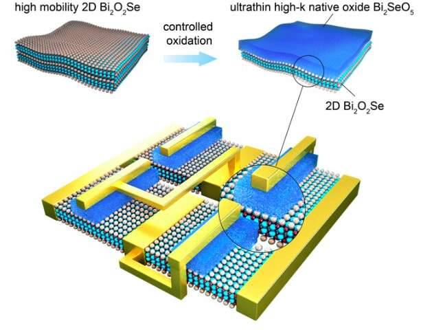
Post Deposition Annealing (PDA) plays a pivotal role in refining the electrical properties of high-k gate dielectrics, which are indispensable for the fabrication of advanced logic and memory devices. This process involves subjecting the deposited high-k materials to elevated temperatures, typically ranging from 300°C to 900°C, to enhance their dielectric constants and reduce leakage currents.
The benefits of PDA are manifold:
- Improved Dielectric Constant: PDA increases the dielectric constant of high-k materials, thereby reducing the equivalent oxide thickness (EOT) without compromising the gate stack's integrity.
- Reduced Leakage Current: By annealing the high-k dielectrics, the density of interface traps is minimized, leading to a significant reduction in leakage currents.
- Enhanced Mobility: PDA can also improve carrier mobility by reducing the scattering effects at the interface between the high-k dielectric and the semiconductor substrate.
| PDA Benefit | Description |
|---|---|
| Improved Dielectric Constant | Increases dielectric constant, reducing EOT without compromising gate stack integrity. |
| Reduced Leakage Current | Minimizes interface traps, significantly reducing leakage currents. |
| Enhanced Mobility | Reduces scattering effects, improving carrier mobility. |
These enhancements are critical for the performance and reliability of modern semiconductor devices, particularly as technology nodes continue to shrink.
Metal Silicide Formation
Optimizing metal silicides through precise annealing conditions is essential for improving device performance. The formation of metal silicides, such as nickel silicide or cobalt silicide, plays a critical role in reducing contact resistance and enhancing the overall efficiency of semiconductor devices. This process involves the controlled interaction of metal layers with silicon substrates, which is highly dependent on the annealing parameters.
The key parameters in this process include the annealing temperature and time. For instance, temperatures typically range from 300°C to 600°C, depending on the specific metal and silicon combination. The duration of the annealing process can vary from a few seconds to several minutes, with rapid thermal annealing (RTA) being a common method due to its ability to achieve precise temperature control and rapid heating and cooling cycles.
| Annealing Method | Temperature Range | Time Duration | Application |
|---|---|---|---|
| RTA | 300°C - 600°C | Seconds | Metal silicide formation |
| Furnace Annealing | 500°C - 950°C | Minutes | General lattice repair and activation |
| FLA | 400°C - 800°C | Milliseconds | Ultra-shallow junctions |
Controlling these parameters ensures that the metal silicides form with the desired properties, such as low resistivity and good thermal stability. This optimization is crucial for the performance of advanced semiconductor devices, particularly in the context of shrinking technology nodes where minimizing resistance and maximizing efficiency are paramount.
Moreover, the choice of annealing technique can significantly impact the quality of the metal silicides. For example, rapid thermal annealing (RTA) allows for precise control over the temperature profile, which is essential for forming high-quality silicides with minimal diffusion of impurities. In contrast, traditional furnace annealing, while effective for broader applications, may not offer the same level of precision required for advanced semiconductor manufacturing.
In summary, the precise control of annealing conditions is vital for the successful formation of metal silicides, which in turn enhances the performance and reliability of semiconductor devices. This optimization is a cornerstone of modern semiconductor manufacturing, particularly as technology nodes continue to shrink and device performance demands increase.
3D Integration Technology
Fast annealing technologies play a pivotal role in the intricate process of 3D integration, particularly in the fabrication of advanced memory devices such as 3D NAND and 3D DRAM. These technologies are essential for optimizing the multiple layers that constitute these complex structures, ensuring that each layer adheres to stringent performance and reliability standards.
In the context of 3D NAND, fast annealing techniques like Rapid Thermal Annealing (RTA) and Flash Lamp Annealing (FLA) are employed to manage the thermal budget efficiently. This is critical for the formation of ultra-shallow junctions, which are necessary to maintain high dopant activation rates while minimizing impurity diffusion. The rapid heating and cooling cycles of these techniques help in precisely controlling the thermal impact on each layer, thereby enhancing the overall device performance.
Similarly, for 3D DRAM, the need for fast annealing is equally paramount. The high-precision thermal treatments provided by these technologies ensure that each layer of the memory stack is densified and optimized. This not only improves the electrical properties of the high-k gate dielectrics but also enhances the reliability and endurance of the memory cells. The ability to control the thermal conditions with high precision allows for the creation of uniform and defect-free layers, which are crucial for the scalability and performance of 3D DRAM devices.
In summary, fast annealing technologies are not just beneficial but indispensable for the successful implementation of 3D integration processes. They enable the precise control of thermal parameters, ensuring that each layer of the 3D structures meets the exacting standards required for modern semiconductor devices.
Related Products
- Controlled Nitrogen Inert Hydrogen Atmosphere Furnace
- Vacuum Heat Treat Furnace with Ceramic Fiber Liner
- High Temperature Muffle Oven Furnace for Laboratory Debinding and Pre Sintering
- Laboratory Muffle Oven Furnace Bottom Lifting Muffle Furnace
- Graphite Vacuum Furnace High Thermal Conductivity Film Graphitization Furnace
Related Articles
- Why Your Brazed Joints Keep Failing: The Invisible Saboteur in Your Furnace
- The Importance of Inert Atmosphere Gases in Furnace Atmospheres
- Hydrogen Atmosphere Furnaces: Applications, Safety, and Maintenance
- How Controlled Atmosphere Furnaces Improve Quality and Consistency in Heat Treatment
- Controlled Atmosphere Furnace: Comprehensive Guide to Advanced Heat Treatment

