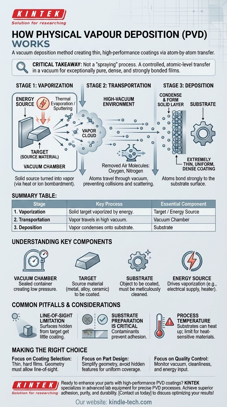
In essence, Physical Vapor Deposition (PVD) is a vacuum deposition method that produces a thin, high-performance coating on a solid part. The process involves three fundamental steps: turning a solid source material into a vapor, transporting that vapor through a vacuum, and then condensing it atom-by-atom onto the surface of the part, known as the substrate.
The critical takeaway is that PVD is not a simple "spraying" process. It is a highly controlled, atomic-level transfer of material inside a vacuum, which is essential for creating a film that is exceptionally pure, dense, and strongly bonded to the surface.
The Three Core Stages of the PVD Process
To understand how PVD works, it is best to break it down into its three sequential stages. Each step is precisely controlled to achieve the desired coating properties.
Stage 1: Vaporization
The process begins with a solid source material, often called a target. This target is placed inside the vacuum chamber and subjected to a highly energetic environment to force atoms or molecules to escape its surface, creating a vapor cloud. This is typically achieved through one of two primary methods: thermal evaporation (heating the material until it vaporizes) or sputtering (bombarding the material with energetic ions).
Stage 2: Transportation
Once vaporized, the atoms of the coating material travel from the target toward the substrate. This journey happens within a high-vacuum environment. This vacuum is not a minor detail; it is fundamental to the entire process.
The vacuum removes air molecules (like oxygen and nitrogen) that would otherwise collide with the traveling atoms. These collisions would cause the atoms to scatter, react, or lose energy, preventing them from ever reaching the substrate or forming a contaminated, low-quality film.
Stage 3: Deposition
When the vaporized atoms reach the cooler substrate, they condense and form a solid layer. This film builds up atom-by-atom, creating an extremely thin, uniform, and dense coating. Because the atoms arrive with significant energy, they lock into a highly structured and strongly adhered film on the substrate's surface.
Understanding the Key Components
Every PVD system is built around a few essential components that enable the process.
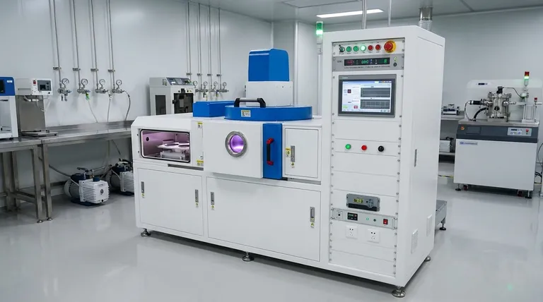
The Vacuum Chamber
This is the sealed container where the entire process takes place. It is pumped down to a very low pressure to create the necessary vacuum environment.
The Target (Source Material)
This is the solid block, powder, or ingot of the material that will become the coating. It can be a pure metal, an alloy, or a ceramic compound like Titanium Nitride.
The Substrate
This is the object or part that is being coated. Substrates are meticulously cleaned before being placed in the chamber to ensure the coating adheres properly.
The Energy Source
This is the mechanism that drives the vaporization stage. In sputtering, this is typically an electrical power supply that creates a plasma of ions. In evaporation, it is a resistive heater or an electron beam that heats the source material.
Common Pitfalls and Considerations
While powerful, PVD is governed by physical principles that create specific limitations. Understanding these is key to successful application.
Line-of-Sight Limitation
Because atoms travel in a relatively straight line from the target to the substrate, PVD is a line-of-sight process. Surfaces that are hidden or shadowed from the target will receive little to no coating. This makes it challenging to coat complex internal geometries without sophisticated part-rotation mechanisms.
Substrate Preparation is Critical
The quality of a PVD coating is entirely dependent on the cleanliness of the substrate. Any microscopic contaminants, such as oils or oxides, will prevent proper adhesion and can cause the film to peel or flake off.
Process Temperature
While the substrate is "cooler" than the vapor source, it is often heated to hundreds of degrees Celsius during the process. This elevated temperature helps improve film density and adhesion but can also be a limitation for heat-sensitive materials like certain plastics or tempered alloys.
Making the Right Choice for Your Goal
Your understanding of the PVD process directly informs how you can apply it.
- If your primary focus is selecting a coating for a part: Recognize that PVD creates a very thin, hard, and durable film, but the part's geometry must allow for line-of-sight access.
- If your primary focus is designing a part for PVD coating: Simplify the geometry where possible, avoiding deep, narrow holes or hidden features to ensure uniform coverage.
- If your primary focus is process quality control: The vacuum level, substrate cleanliness, and energy input are the three most critical parameters to monitor.
By understanding these core principles of vaporization, transport, and deposition, you can effectively diagnose issues and leverage PVD technology for its intended purpose.
Summary Table:
| Stage | Key Process | Essential Component |
|---|---|---|
| 1. Vaporization | Solid target material is vaporized using heat or sputtering. | Target / Energy Source |
| 2. Transportation | Vapor travels through a high-vacuum environment. | Vacuum Chamber |
| 3. Deposition | Vapor condenses atom-by-atom onto the substrate surface. | Substrate |
Ready to enhance your parts with high-performance PVD coatings?
KINTEK specializes in advanced lab equipment and consumables for precise PVD processes. Our solutions help you achieve superior coating adhesion, purity, and durability for your laboratory or manufacturing needs.
Contact us today to discuss how our expertise can optimize your coating results!
Visual Guide
Related Products
- Chemical Vapor Deposition CVD Equipment System Chamber Slide PECVD Tube Furnace with Liquid Gasifier PECVD Machine
- RF PECVD System Radio Frequency Plasma-Enhanced Chemical Vapor Deposition RF PECVD
- 915MHz MPCVD Diamond Machine Microwave Plasma Chemical Vapor Deposition System Reactor
- HFCVD Machine System Equipment for Drawing Die Nano-Diamond Coating
- Customer Made Versatile CVD Tube Furnace Chemical Vapor Deposition Chamber System Equipment
People Also Ask
- How expensive is chemical vapor deposition? Understanding the True Cost of High-Performance Coating
- How are carbon nanotubes grown? Master Scalable Production with Chemical Vapor Deposition
- What are the processes of vapor phase deposition? Understand CVD vs. PVD for Superior Thin Films
- What is the chemical vapor deposition growth process? Build Superior Thin Films from the Atom Up
- What is plasma enhanced chemical vapor deposition PECVD equipment? A Guide to Low-Temperature Thin Film Deposition


