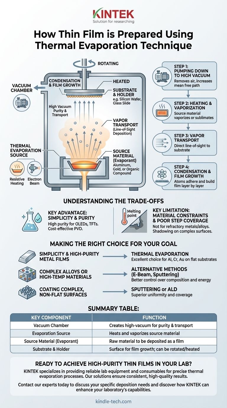
In essence, thermal evaporation prepares a thin film by heating a source material inside a high-vacuum chamber until it vaporizes. This vapor then travels and condenses onto a cooler surface, called a substrate, building up a thin, uniform layer atom by atom.
The core principle of thermal evaporation is a controlled phase transition: a solid material is turned into a gas and then back into a solid on a new surface. The high vacuum is the critical element that ensures the material travels from source to substrate without contamination or interference.
The Anatomy of a Thermal Evaporation System
To understand the process, you must first understand its essential components. Each part plays a critical role in controlling the quality and characteristics of the final film.
The Vacuum Chamber
The entire process takes place within a sealed chamber, typically made of stainless steel. Its purpose is to create a high-vacuum environment, which is essential for two reasons: purity and transport. It removes atmospheric gases that could react with and contaminate the film, and it allows vaporized atoms to travel directly to the substrate without colliding with other particles.
The Evaporation Source
This is the heart of the system, responsible for holding and heating the material. The source is usually a "boat" or "crucible" made from a refractory material with a very high melting point, like tungsten or molybdenum.
Heating is achieved in one of two primary ways:
- Resistive Heating: A large electrical current is passed through the boat itself, causing it to heat up like a filament in a light bulb, which in turn melts or sublimates the source material within it.
- Electron Beam (E-Beam): A high-energy beam of electrons is fired at the source material, transferring immense energy to a very localized spot and causing it to vaporize.
The Source Material (Evaporant)
This is the raw material you intend to deposit, such as aluminum, gold, or an organic compound. It is placed inside the crucible or boat before the process begins.
The Substrate and Holder
The substrate is the surface onto which the thin film is grown (e.g., a silicon wafer, glass slide, or polymer). It is positioned above the evaporation source on a dedicated holder. This holder can often be rotated to ensure the film deposits evenly across the entire surface and may also be heated to improve the film's adhesion and crystalline structure.
The Step-by-Step Deposition Process
The creation of a thin film via thermal evaporation follows a precise, four-stage sequence.
Step 1: Pumping Down to High Vacuum
First, the chamber is sealed and pumps are used to remove the air, reducing the internal pressure to a high vacuum. This increases the mean free path—the average distance an atom can travel before hitting another atom—ensuring a direct line-of-sight path from the source to the substrate.
Step 2: Heating and Vaporization
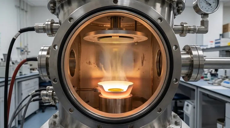
Once the target vacuum is reached, the heating system is activated. The source material is heated until its vapor pressure becomes significant, causing it to evaporate (for liquids) or sublimate (for solids). A cloud of vapor begins to fill the area around the source.
Step 3: Vapor Transport
Due to the high vacuum, the vaporized atoms or molecules travel outwards from the source in straight lines. This is a crucial characteristic known as line-of-sight deposition.
Step 4: Condensation and Film Growth
When the energetic vapor atoms strike the relatively cooler substrate, they lose their energy, condense back into a solid state, and stick to the surface. Over time, millions of these atoms accumulate, growing layer by layer to form the desired thin film.
Understanding the Trade-offs
While powerful, thermal evaporation is not a universal solution. Understanding its advantages and limitations is key to using it effectively.
Key Advantage: Simplicity and Purity
Thermal evaporation is a relatively simple and cost-effective form of Physical Vapor Deposition (PVD). Because it operates in a high vacuum and doesn't use process gases, it can produce films of very high purity, which is critical for applications like OLEDs and thin-film transistors.
Key Limitation: Material Constraints
This method works best for materials with relatively low melting or sublimation points. It is not well-suited for depositing refractory metals with very high melting points or complex alloys, as the different elements in the alloy may evaporate at different rates, changing the film's final composition.
Key Limitation: Poor Step Coverage
The line-of-sight nature of the deposition means it cannot uniformly coat surfaces with complex, three-dimensional topography. Areas not in the direct line of sight of the source will receive little to no coating, an effect known as "shadowing."
Making the Right Choice for Your Goal
Selecting the correct deposition technique depends entirely on your material and the desired film properties.
- If your primary focus is simplicity and high-purity metal films: Thermal evaporation is an excellent and widely used choice for depositing materials like aluminum, chromium, or gold onto flat substrates.
- If your primary focus is depositing complex alloys or high-temperature materials: You should consider alternative methods like electron-beam evaporation or sputtering, which offer better control over composition and energy.
- If your primary focus is coating complex, non-flat surfaces: The line-of-sight limitation is critical. Techniques like sputtering or atomic layer deposition (ALD) will provide far superior uniformity and coverage.
By understanding these core principles, you can effectively leverage thermal evaporation to create high-quality thin films tailored to your specific application.
Summary Table:
| Key Component | Function | Common Materials |
|---|---|---|
| Vacuum Chamber | Creates a high-vacuum environment for purity and transport | Stainless steel |
| Evaporation Source | Heats and vaporizes the source material | Tungsten, Molybdenum (boats/crucibles) |
| Source Material (Evaporant) | The raw material to be deposited as a film | Aluminum, Gold, Chromium |
| Substrate & Holder | Surface for film growth; can be rotated/heated | Silicon wafers, glass slides |
Ready to achieve high-purity thin films in your lab?
KINTEK specializes in providing reliable lab equipment and consumables for precise thermal evaporation processes. Whether you are depositing metals for electronics or researching new materials, our solutions ensure consistent, high-quality results.
Contact our experts today to discuss your specific deposition needs and discover how KINTEK can enhance your laboratory's capabilities.
Visual Guide
Related Products
- Molybdenum Tungsten Tantalum Evaporation Boat for High Temperature Applications
- Aluminized Ceramic Evaporation Boat for Thin Film Deposition
- Evaporation Boat for Organic Matter
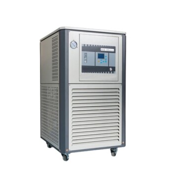
- 5L Heating Chilling Circulator Cooling Water Bath Circulator for High and Low Temperature Constant Temperature Reaction
- 20L Heating Chilling Circulator Cooling Water Bath Circulator for High and Low Temperature Constant Temperature Reaction
People Also Ask
- What is the thermal evaporation method in thin film? A Guide to Simple, Cost-Effective PVD
- What is the widely used boat made of in thermal evaporation? Choosing the Right Material for High-Purity Deposition
- What are thermal evaporation sources? Key Types and How to Choose the Right One
- How does a molybdenum evaporation source function in H2S for MoS2 synthesis? Master Reactive Film Deposition
- What is the source of evaporation for thin film? Choosing Between Thermal and E-Beam Methods