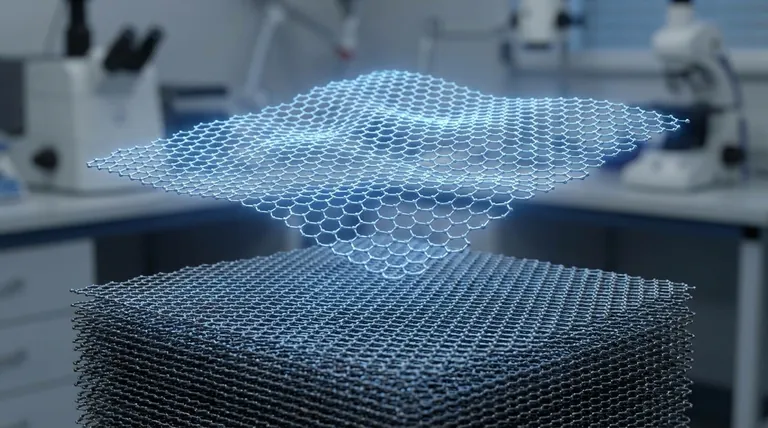
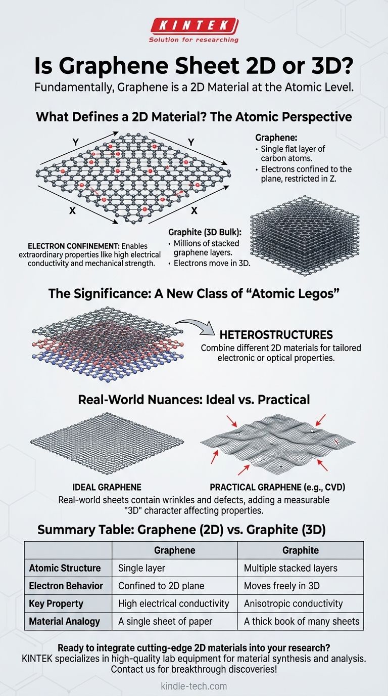
Fundamentally, graphene is a two-dimensional (2D) material. While any physical sheet exists in three-dimensional space, its classification as "2D" refers to its structure at the atomic level. Graphene is a single, flat layer of carbon atoms arranged in a honeycomb lattice, making it the thinnest material ever created.
The term "2D material" describes a substance that is a single atomic or molecular layer thick. This extreme confinement to a plane is what gives materials like graphene their extraordinary electronic and mechanical properties, which are fundamentally different from their 3D bulk counterparts.
What Defines a "2D Material"?
The distinction between 2D and 3D is not about how we perceive an object in our world, but about its behavior at the quantum scale.
The Atomic-Scale Perspective
A true 2D material consists of a single plane of atoms. For graphene, this is a layer of carbon atoms bonded together.
Its 3D equivalent is graphite—the material found in pencils—which is simply millions of graphene sheets stacked on top of one another.
The Critical Role of Electron Confinement
The most important consequence of this structure is electron confinement. In a 2D material, electrons can move freely across the plane (in the X and Y directions) but their movement is heavily restricted in the third dimension (Z).
This confinement is not just a geometric curiosity; it dramatically changes the physics of the material, enabling properties like exceptionally high electrical conductivity and mechanical strength.
The Significance of the 2D Classification
Understanding graphene as a 2D material is key to grasping why it has generated so much excitement in science and engineering.
A New Class of Materials
Graphene was the first true 2D material to be isolated, proving that such structures could be stable. Its discovery opened the door to an entire family of other 2D materials.
As noted in research, materials like boron nitride (an insulator) and transition metal dichalcogenides (TMDs) offer a wide range of properties, such as tunable bandgaps, that are not available in graphene.
The "Atomic Legos" Concept
The true potential is realized when these different 2D materials are combined. Scientists can stack different layers on top of one another to create entirely new, man-made materials called heterostructures.
This "Atomic Legos" approach allows for the engineering of materials with precisely tailored electronic or optical properties, designed for a specific purpose.
Understanding the Real-World Nuances
While theoretically perfect, real-world graphene sheets have complexities that must be acknowledged.
Ideal vs. Practical Graphene
A perfect graphene sheet is perfectly flat. However, large-area sheets produced through methods like Chemical Vapor Deposition (CVD) are never perfectly flat.
They contain wrinkles, ripples, and defects. These features add a small but measurable "third-dimensional" character that can influence the material's overall properties and must be accounted for in device engineering.
The Challenge of Synthesis
The very nature of a 2D material makes it incredibly delicate. Producing large, high-quality, single-layer sheets without defects remains a significant manufacturing challenge that the field is actively working to solve.
How to Think About Graphene's Dimensionality
Your perspective on graphene's dimensionality depends on your objective.
- If your primary focus is on fundamental physics: Treat graphene as a pure 2D system to understand its unique electronic behavior.
- If your primary focus is on device engineering: Acknowledge its 2D atomic nature but also account for the real-world 3D characteristics like wrinkles and defects during fabrication.
Understanding this distinction between the ideal 2D model and its practical 3D reality is the key to unlocking its revolutionary potential.
Summary Table:
| Aspect | Graphene (2D) | Graphite (3D Bulk) |
|---|---|---|
| Atomic Structure | Single layer of carbon atoms | Multiple stacked graphene layers |
| Electron Behavior | Confined to 2D plane (X, Y) | Moves freely in all three dimensions |
| Key Property | Exceptionally high electrical conductivity | Anisotropic conductivity (varies by direction) |
| Material Analogy | A single sheet of paper | A thick book made of many paper sheets |
Ready to integrate cutting-edge 2D materials like graphene into your research? KINTEK specializes in providing high-quality lab equipment and consumables tailored for advanced material synthesis and analysis. Whether you're working with CVD systems for graphene growth or characterizing novel heterostructures, our expertise ensures you have the reliable tools needed for breakthrough discoveries. Contact our team today to discuss how we can support your laboratory's specific needs!
Visual Guide
Related Products
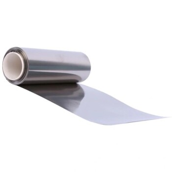
- High-Purity Titanium Foil and Sheet for Industrial Applications
- High Temperature Resistant Optical Quartz Glass Sheet
- Custom PTFE Teflon Parts Manufacturer for PTFE Mesh F4 Sieve
- Nickel Foam for Industrial and Laboratory Applications
- Platinum Sheet Electrode for Laboratory and Industrial Applications
People Also Ask
- What are the disadvantages of using metal? Understanding Corrosion, Weight, and Cost Challenges
- How does hardness change with temperature? Understand the Inverse Relationship to Prevent Failure
- What is titanium used for in manufacturing? Leveraging High-Performance Properties for Critical Applications
- How can you improve corrosion resistance? Extend Equipment Life with Proven Strategies
- What is the difference between metallic and non-metallic coating? A Guide to Sacrificial vs. Barrier Protection