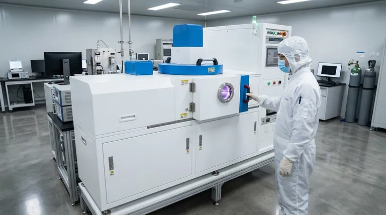
At its core, RF sputtering is a thin-film deposition technique primarily used for materials that are electrical insulators or semiconductors. Its most common applications are found in the manufacturing of microelectronics, from complex computer chips to optical coatings, where depositing uniform, high-quality layers of non-conductive materials is essential.
The fundamental reason to use RF sputtering is to overcome a critical limitation of simpler methods like DC sputtering. It allows you to deposit insulating materials without the process-halting charge buildup that occurs with direct current, unlocking a wide range of advanced applications.
The Core Problem RF Sputtering Solves
To understand the applications of RF sputtering, you must first understand the problem it was designed to fix. The key lies in the electrical properties of the material you wish to deposit.
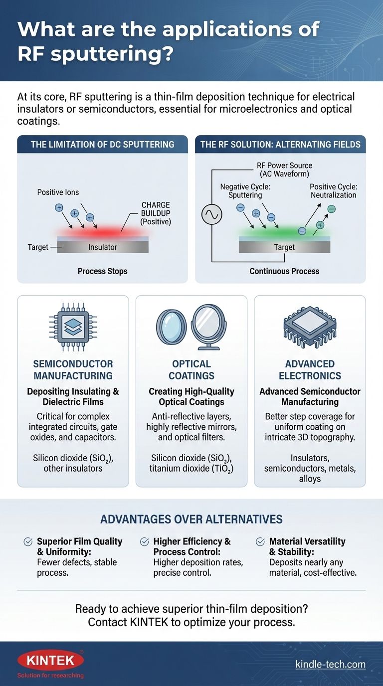
The Limitation of DC Sputtering
In standard DC (Direct Current) sputtering, a target material is bombarded by positive ions from a plasma to "sputter" atoms onto a substrate. This works exceptionally well for electrically conductive materials, like metals.
However, if the target material is an insulator (a dielectric), the positive ions stick to its surface. This causes a rapid positive charge buildup, which electrically repels any more incoming positive ions and effectively stops the sputtering process.
The RF Solution: Alternating Fields
RF (Radio Frequency) sputtering solves this by replacing the DC power source with a high-frequency AC source. This field rapidly alternates between positive and negative potential.
During the negative cycle, positive ion bombardment sputters the material as intended. During the brief positive cycle, the target attracts a shower of electrons from the plasma, which neutralizes the positive charge built up on the surface. This prevents charge buildup and allows for the continuous, stable deposition of insulating materials.
Key Capabilities and Applications
This ability to handle non-conductive materials is the foundation for RF sputtering's primary applications.
Depositing Insulating and Dielectric Films
The most important application is the creation of thin insulating layers. This is critical in the semiconductor industry for building the complex, layered structures of integrated circuits.
These dielectric films are used to isolate conductive components, form the gate oxides in transistors, and create capacitors directly on a chip.
Creating High-Quality Optical Coatings
RF sputtering is used to deposit precise layers of materials like silicon dioxide (SiO₂) or titanium dioxide (TiO₂) onto glass.
These films are used to create anti-reflective coatings for lenses, highly reflective mirrors, and optical filters where film uniformity and purity are paramount.
Advanced Semiconductor Manufacturing
Compared to other methods, RF sputtering operates at lower pressures (1-15 mTorr). This reduces the chance of sputtered atoms colliding with gas molecules on their way to the substrate.
The result is a more direct path and better "step coverage," meaning the film can uniformly coat the intricate, three-dimensional topography of a modern microchip. This leads to higher quality and more reliable devices.
Understanding the Advantages Over Alternatives
Choosing RF sputtering is a technical decision driven by its distinct advantages in specific scenarios, particularly when compared to DC sputtering or thermal evaporation.
Superior Film Quality and Uniformity
The AC field prevents the arcing and charge buildup that plague DC sputtering of certain materials. This leads to a more stable process and results in films with fewer defects and greater uniformity across the entire substrate.
Higher Efficiency and Process Control
RF energy is very effective at sustaining a plasma, even at low pressures. This increases the density of ions available for sputtering, leading to higher deposition rates compared to DC sputtering at the same low pressure.
This gives engineers precise control over the film's growth and properties.
Material Versatility and Stability
RF sputtering is not limited to insulators; it can deposit nearly any material, including metals, alloys, and composites. Modern developments like RF diode sputtering have further improved the process by eliminating issues like uneven target erosion ("race track" effect), leading to a more stable, repeatable, and cost-effective manufacturing process.
Making the Right Choice for Your Goal
The decision to use RF sputtering hinges on the material you need to deposit and the quality you require for the final film.
- If your primary focus is cost-effective deposition of conductive metals: Standard DC sputtering is often the more economical and straightforward choice.
- If your primary focus is depositing any insulating, dielectric, or semiconductor material: RF sputtering is not just an option; it is the necessary technology.
- If your primary focus is achieving the highest film quality, uniformity, and step coverage for complex devices: RF sputtering provides superior process stability and control for mission-critical applications.
Ultimately, choosing RF sputtering is a choice for versatility and quality, enabling the fabrication of the advanced materials that power our modern electronic world.
Summary Table:
| Application Area | Key Use Case | Materials Deposited |
|---|---|---|
| Semiconductor Manufacturing | Dielectric layers, gate oxides, capacitors | Silicon dioxide (SiO₂), other insulators |
| Optical Coatings | Anti-reflective layers, mirrors, filters | Silicon dioxide (SiO₂), titanium dioxide (TiO₂) |
| Advanced Electronics | Uniform film deposition on complex 3D structures | Insulators, semiconductors, metals, alloys |
Ready to achieve superior thin-film deposition for your lab?
RF sputtering is essential for depositing insulating and dielectric materials with high uniformity and precision. Whether you're developing advanced semiconductors, optical coatings, or complex electronic devices, KINTEK's expertise in lab equipment and consumables can help you optimize your process.
Our solutions are designed to provide the stability, control, and material versatility your projects demand. Contact us today to discuss how we can support your laboratory's specific needs and help you achieve exceptional results.
Get in touch with our experts now!
Visual Guide
Related Products
- RF PECVD System Radio Frequency Plasma-Enhanced Chemical Vapor Deposition RF PECVD
- HFCVD Machine System Equipment for Drawing Die Nano-Diamond Coating
- 915MHz MPCVD Diamond Machine Microwave Plasma Chemical Vapor Deposition System Reactor
- Chemical Vapor Deposition CVD Equipment System Chamber Slide PECVD Tube Furnace with Liquid Gasifier PECVD Machine
- Split Chamber CVD Tube Furnace with Vacuum Station Chemical Vapor Deposition System Equipment Machine
People Also Ask
- How does Radio Frequency Enhanced Plasma Chemical Vapour Deposition (RF-PECVD) work? Learn the Core Principles
- How does plasma enhance CVD? Unlock Low-Temperature, High-Quality Film Deposition
- What is plasma enhanced chemical vapour deposition process? Unlock Low-Temperature, High-Quality Thin Films
- What is plasma chemical vapor deposition? A Low-Temperature Thin Film Coating Solution
- What is the role of RF-PECVD in VFG preparation? Mastering Vertical Growth and Surface Functionality


