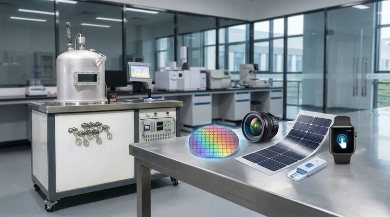
In short, thin film applications are the invisible foundation of virtually all modern technology. These ultra-thin layers of material, often just a few atoms thick, are responsible for the function of everything from the microprocessors in your computer and the anti-glare coating on your glasses to advanced solar panels and life-saving medical sensors.
The core purpose of a thin film is to give a bulk material a new surface property it doesn't naturally possess. This simple principle is the key to enabling the performance, efficiency, and miniaturization that defines modern electronics, optics, and energy systems.
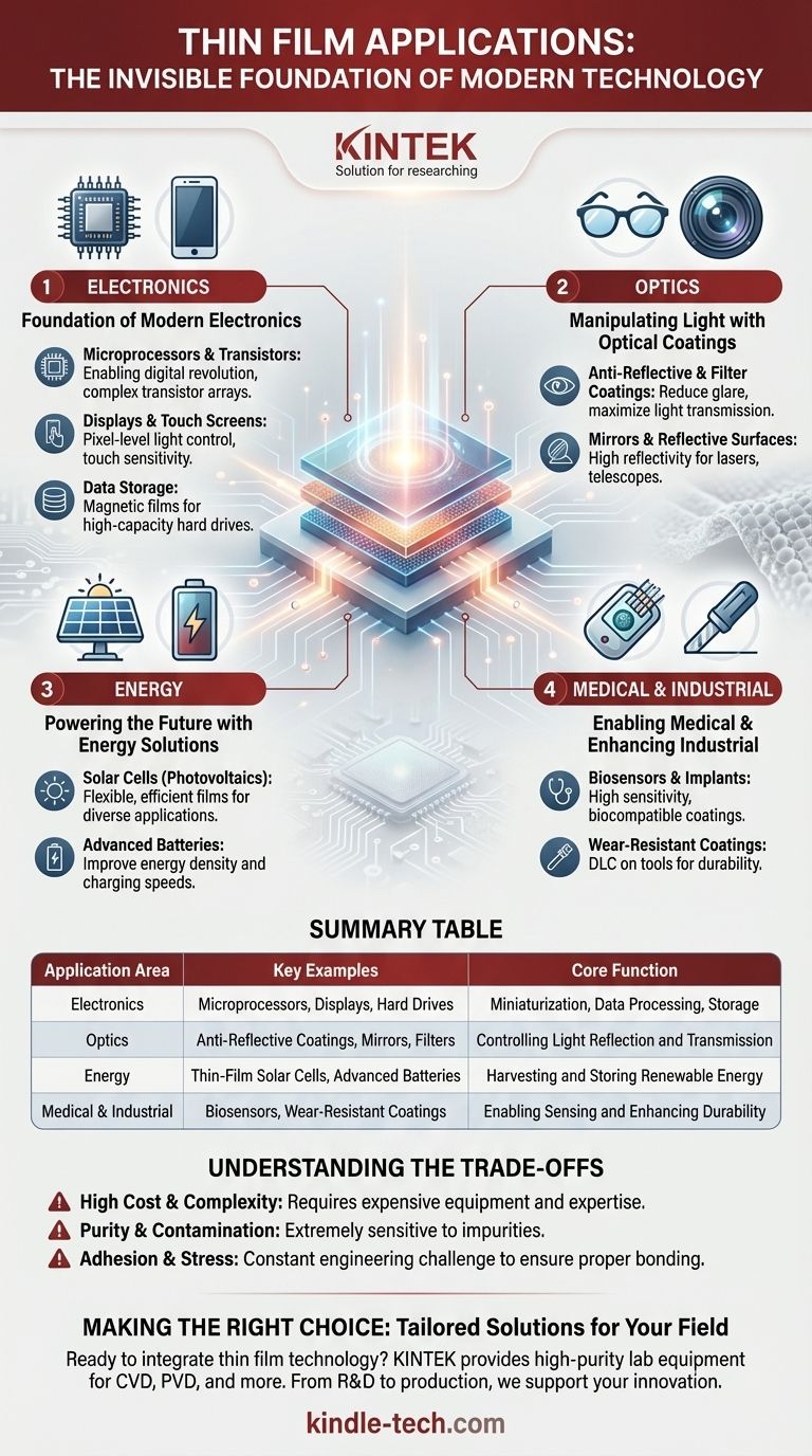
The Foundation of Modern Electronics
The most significant impact of thin film technology is in the semiconductor industry. Without the ability to deposit and etch precise, ultra-pure thin films, the digital revolution would not have been possible.
Semiconductors and Microprocessors
Thin films are the building blocks of transistors, the microscopic switches that form the basis of all computer chips. Processes like Chemical Vapor Deposition (CVD) and Physical Vapor Deposition (PVD) are used to build up complex transistor arrays layer by layer, creating the microprocessors that power our laptops and phones.
Displays and Touch Screens
The vibrant flat-panel displays on televisions, tablets, and smartphones rely on thin films. These layers control light and color at a pixel level, while transparent conductive films create the touch-sensitive screens we use every day.
Data Storage
Modern memory and data storage also depend on thin film technology. Magnetic films are deposited onto platters to create hard drives, enabling the storage of vast amounts of digital information.
Manipulating Light with Optical Coatings
Thin films give engineers precise control over how light interacts with a surface, leading to a wide range of optical applications.
Anti-Reflective and Filter Coatings
The coating on your eyeglasses or a camera lens is a thin film designed to reduce reflection and glare, maximizing light transmission. Other films can be designed to filter specific wavelengths of light, a crucial function in scientific instruments and sensors.
Mirrors and Reflective Surfaces
The classic "silvering" process for creating a mirror is a form of thin film deposition. Highly reflective films are also used in advanced applications like lasers and telescopes to direct light with minimal loss.
Powering the Future with Energy Solutions
Thin film technology is at the forefront of renewable energy and energy storage, offering more efficient and versatile solutions.
Solar Cells (Photovoltaics)
Thin-film solar cells are a major innovation in solar energy. These films can be deposited on flexible materials, opening up applications beyond traditional rooftop panels, such as power-generating tiles or even windows.
Advanced Batteries
The performance and capacity of modern batteries are heavily influenced by the thin films used on their electrodes and separators. This technology is critical for improving energy density and charging speeds in everything from electric vehicles to consumer electronics.
Understanding the Trade-offs
While powerful, thin film deposition is a highly specialized process with inherent complexities that create specific trade-offs.
High Cost and Complexity
The equipment required, such as vacuum deposition chambers, is expensive to acquire and operate. The processes demand precise control over temperature, pressure, and gas chemistry, requiring significant technical expertise.
Purity and Contamination Control
Thin film processes are extremely sensitive to impurities. The entire manufacturing environment, from the raw precursor materials to the processing chamber, must be kept impeccably clean to avoid defects that can ruin a device.
Adhesion and Stress
Ensuring a thin film properly adheres to the underlying substrate without cracking or peeling is a constant engineering challenge. Mismatches in material properties can build up internal stress, leading to device failure.
Making the Right Choice for Your Field
The application of thin films is always tailored to a specific goal. Understanding your priority helps clarify why this technology is chosen.
- If your primary focus is consumer electronics: Thin films are the key to miniaturization, processing speed, and display quality in devices like phones and computers.
- If your primary focus is industrial performance: Thin films provide critical surface properties, such as the wear resistance of diamond-like carbon (DLC) on cutting tools.
- If your primary focus is energy and sustainability: Thin films are essential for creating next-generation solar cells and high-capacity batteries.
- If your primary focus is medical technology: Thin films enable the development of highly sensitive biosensors and biocompatible coatings for implants.
Ultimately, thin film technology is a masterclass in how controlling materials at the nanoscale creates immense value at the macro scale.
Summary Table:
| Application Area | Key Examples | Core Function |
|---|---|---|
| Electronics | Microprocessors, Displays, Hard Drives | Miniaturization, Data Processing, Storage |
| Optics | Anti-Reflective Coatings, Mirrors, Filters | Controlling Light Reflection and Transmission |
| Energy | Thin-Film Solar Cells, Advanced Batteries | Harvesting and Storing Renewable Energy |
| Medical & Industrial | Biosensors, Wear-Resistant Coatings | Enabling Sensing and Enhancing Durability |
Ready to integrate thin film technology into your lab's research or production? KINTEK specializes in providing the high-purity lab equipment and consumables essential for reliable thin film deposition processes like CVD and PVD. Whether you're developing next-generation electronics, advanced optics, or sustainable energy solutions, our expertise supports your innovation from R&D to production.
Contact our experts today to discuss how we can meet your specific laboratory needs.
Visual Guide
Related Products
- Aluminum-Plastic Flexible Packaging Film for Lithium Battery Packaging
- Thin-Layer Spectral Electrolysis Electrochemical Cell
People Also Ask
- What is the thinnest coating? Unlocking Unique Properties at the Atomic Scale
- How is aluminum foil utilized as a consumable during the assembly of cold sintering molds? Optimize Tooling Longevity
- What are the three types of lamination? Choose the Perfect Finish for Your Print Project
- What is the difference between single layer film and multi layer film? A Guide to Material Selection
- How to tell if a lithium-ion battery is bad? Spot the critical signs of failure before it's too late.

