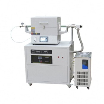
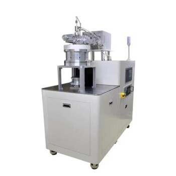
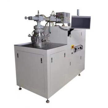
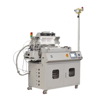
PECVD systems serve as the critical infrastructure for depositing thin films when standard thermal processes would damage the device. In the semiconductor industry, their primary applications are the fabrication of microelectronic devices, photovoltaic cells, and display panels, specifically through the creation of foundational layers like silicon nitride and silicon dioxide.
Core Takeaway PECVD (Plasma Enhanced Chemical Vapor Deposition) is the definitive solution for depositing high-quality insulating and conducting films on temperature-sensitive substrates. It allows manufacturers to create essential layers for Integrated Circuits (ICs), Thin-Film Transistors (TFTs), and solar cells without subjecting the device to the destructive high heat associated with traditional CVD methods.
Semiconductor Device Fabrication
PECVD is indispensable in the creation of modern integrated circuits (ICs) where precision and thermal management are paramount.
Integrated Circuit (IC) Dielectrics
PECVD is widely used to deposit dielectric layers, such as silicon dioxide (SiO2) and silicon nitride (SiNx). These layers act as electrical insulation between conductive parts of a chip, preventing short circuits and ensuring signal integrity.
Low-k Dielectric Materials
For advanced chip manufacturing, PECVD systems deposit low-k dielectric materials. These materials reduce parasitic capacitance in high-speed circuits, which is essential for improving the performance and processing speed of modern processors.
Thin-Film Transistors (TFTs)
A major application of PECVD is the production of Thin-Film Transistors (TFTs). By depositing amorphous silicon (a-Si:H) and other foundational materials, these systems create the switching components required for pixel control in modern display technologies.
Energy and Large-Area Electronics
Beyond microscopic chips, PECVD is uniquely capable of handling large surface areas, making it vital for the energy and display sectors.
Photovoltaic Cells (Solar Panels)
In the solar industry, PECVD is used to coat large panels with uniform thin films. These films are critical for the energy conversion efficiency of solar cells, creating the active layers that capture sunlight and convert it into electricity.
Display Panel Manufacturing
The technology is extensively utilized to fabricate the backplanes of flat-panel displays. The ability to deposit uniform films over large glass substrates ensures consistent brightness and color quality across television and monitor screens.
Specialized Industrial and Optical Coatings
The versatility of plasma allows PECVD to extend into fields requiring specific mechanical or optical properties.
Wear-Resistant Coatings (Tribology)
PECVD is used to produce Diamond-like Carbon (DLC). This coating provides exceptional hardness and low friction, utilized in applications ranging from mechanical parts requiring wear resistance to biomedical implants.
Optical Layer Tuning
Manufacturers use PECVD to finely tune the refractive index of optical layers. By adjusting the plasma parameters, engineers can create specialized coatings for precision optics, photometers, and even consumer goods like sunglasses.
Understanding the Trade-offs
While PECVD is a powerful tool, it is selected based on specific engineering constraints regarding temperature.
The Thermal Constraint
The primary reason engineers choose PECVD over methods like Low-Pressure CVD (LPCVD) or thermal oxidation is temperature sensitivity.
If a substrate or a previously deposited layer cannot withstand high thermal cycles, PECVD is the mandatory choice. However, if the materials are robust enough to handle high heat, other thermal methods might be considered for different film density characteristics.
Making the Right Choice for Your Goal
- If your primary focus is Integrated Circuits: Prioritize PECVD for depositing low-k dielectrics and passivation layers that require precise thickness control at lower temperatures.
- If your primary focus is Display or Solar Technology: Leverage PECVD for its ability to maintain high uniformity across very large surface areas, essential for TFT backplanes and photovoltaic panels.
- If your primary focus is Mechanical Durability: utilize PECVD to deposit Diamond-like Carbon (DLC) for superior wear resistance on tools or medical implants.
PECVD is the bridge that allows high-performance materials to be integrated into devices that cannot survive the heat of traditional manufacturing.
Summary Table:
| Application Category | Primary Materials | Key Industry Use |
|---|---|---|
| Semiconductor ICs | Silicon Dioxide (SiO2), Silicon Nitride (SiNx) | Electrical insulation and low-k dielectrics |
| Display Technology | Amorphous Silicon (a-Si:H) | Thin-Film Transistors (TFTs) for flat panels |
| Photovoltaics | Silicon-based thin films | Active layers for solar cell energy conversion |
| Mechanical/Optical | Diamond-like Carbon (DLC) | Wear-resistant coatings and optical tuning |
Elevate Your Semiconductor Research and Production
Precise thin-film deposition is the backbone of modern electronics. At KINTEK, we understand that thermal sensitivity shouldn't compromise your material quality. Whether you are developing next-generation integrated circuits, high-efficiency photovoltaic cells, or advanced display panels, our specialized PECVD systems and CVD equipment provide the uniformity and control your lab requires.
From high-temperature furnaces to precision crushing and milling systems, KINTEK offers a comprehensive suite of laboratory equipment and consumables tailored for target industries like battery research and material science.
Ready to optimize your deposition process?
Contact KINTEK today to find the perfect system for your application!
Related Products
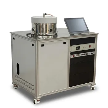
- RF PECVD System Radio Frequency Plasma-Enhanced Chemical Vapor Deposition RF PECVD
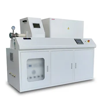
- Chemical Vapor Deposition CVD Equipment System Chamber Slide PECVD Tube Furnace with Liquid Gasifier PECVD Machine
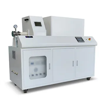
- Inclined Rotary Plasma Enhanced Chemical Vapor Deposition PECVD Equipment Tube Furnace Machine
- Inclined Rotary Plasma Enhanced Chemical Vapor Deposition PECVD Equipment Tube Furnace Machine
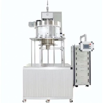
- 915MHz MPCVD Diamond Machine Microwave Plasma Chemical Vapor Deposition System Reactor
People Also Ask
- What is an example of PECVD? RF-PECVD for High-Quality Thin Film Deposition
- What is plasma CVD? Unlock Low-Temperature Thin Film Deposition for Sensitive Materials
- What is the role of RF-PECVD in VFG preparation? Mastering Vertical Growth and Surface Functionality
- How does plasma enhance CVD? Unlock Low-Temperature, High-Quality Film Deposition
- Why is a Matching Network Indispensable in RF-PECVD for Siloxane Films? Ensure Stable Plasma and Uniform Deposition

