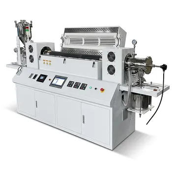
High-capacity tubular PECVD equipment is engineered specifically to lower manufacturing costs for the crystalline silicon market by maximizing throughput without sacrificing quality. These systems feature a massive processing architecture, utilizing five process tubes per unit with each tube accommodating 400 wafers (156-162mm), allowing a single machine to support a production line capacity of over 110MW.
Core Insight: The defining value of this equipment is its ability to decouple volume from cost. It achieves economies of scale through high-density loading while maintaining the strict film uniformity required for efficient solar energy conversion.
Throughput and Capacity Architecture
The primary design philosophy behind this equipment is the maximization of volume per footprint.
Multi-Tube Configuration
Unlike standard units that may operate with fewer chambers, high-capacity models integrate five process tubes into a single piece of equipment.
This consolidation reduces the physical footprint required on the factory floor while significantly increasing output potential.
High-Density Wafer Loading
Each individual tube is engineered to process 400 wafers simultaneously.
This capacity applies to standard wafer sizes ranging from 156mm to 162mm, ensuring compatibility with current market standards for crystalline silicon cells.
Production Line Support
Because of this high-density architecture, a single unit can anchor a production line with an output exceeding 110MW.
This capability allows manufacturers to scale operations rapidly with fewer total machines, directly addressing the industry's need for lower capital expenditure per watt.
Film Quality and Process Precision
High capacity is valuable only if the resulting film quality remains consistent. This equipment utilizes specific mechanisms to ensure performance does not degrade at scale.
Uniformity Control
Despite the high volume, the equipment maintains good film formation uniformity, a critical metric for solar cell efficiency.
This is achieved through a vacuum-sealed tube furnace, which minimizes impurities and ensures consistent environmental conditions across the large batch of wafers.
Thermal and Adhesion Efficiency
The system relies on a uniform temperature within the reaction zone to accelerate reaction speeds without compromising the film structure.
Simultaneously, the plasma generator creates high-energy plasma, ensuring the deposited film bonds strongly to the substrate (high adhesion) while mitigating internal stress.
Understanding the Trade-offs
While high-capacity tubular PECVD offers significant cost advantages, it introduces specific operational considerations.
The "All-in-One" Risk
Concentrating production into large, multi-tube units creates a single point of failure. If the central vacuum or temperature control system fails, production stops for all five tubes simultaneously, potentially halting 110MW worth of throughput.
Complexity of Uniformity
Maintaining uniformity across 2,000 wafers (5 tubes x 400 wafers) is technically more demanding than processing smaller batches.
Operators must ensure rigorous maintenance of the vacuum system and plasma generators, as minor deviations in the reaction zone can affect a significantly larger volume of product.
Making the Right Choice for Your Goal
When integrating this equipment into a manufacturing line, consider your primary operational objectives.
- If your primary focus is Cost Reduction: Leverage the 110MW+ capacity of a single unit to minimize factory footprint and overhead, but ensure you have a robust preventative maintenance schedule to avoid costly downtime.
- If your primary focus is Process Consistency: Monitor the vacuum levels and temperature uniformity closely; these are the mechanisms that allow you to process 400 wafers per tube without sacrificing film adhesion or quality.
Summary: High-capacity tubular PECVD is the strategic choice for manufacturers aiming to drive down the cost of crystalline silicon cells by balancing massive batch sizes with precise environmental controls.
Summary Table:
| Feature | Specification/Benefit |
|---|---|
| Processing Architecture | 5 Process Tubes per unit |
| Wafer Capacity | 400 wafers (156-162mm) per tube |
| Total Production Output | >110MW line capacity support |
| Film Quality | High uniformity and adhesion via vacuum-sealed furnaces |
| Key Mechanisms | High-energy plasma deposition and uniform thermal zones |
Optimize Your Solar Cell Production with KINTEK
Are you looking to reduce manufacturing costs while maintaining peak film quality? KINTEK specializes in advanced laboratory and industrial equipment, including high-performance high-temperature furnaces, PECVD systems, and vacuum solutions tailored for the crystalline silicon market. Our expertise in thermal precision and vacuum-sealed environments ensures your materials achieve the uniformity required for high-efficiency solar energy conversion.
From high-capacity tubular furnaces to specialized ceramics and crucibles, we provide the comprehensive tools needed for cutting-edge battery and solar research. Contact KINTEK today to discover how our high-throughput solutions can scale your production line to 110MW and beyond!
Related Products
- Inclined Rotary Plasma Enhanced Chemical Vapor Deposition PECVD Equipment Tube Furnace Machine
- Chemical Vapor Deposition CVD Equipment System Chamber Slide PECVD Tube Furnace with Liquid Gasifier PECVD Machine
- Inclined Rotary Plasma Enhanced Chemical Vapor Deposition PECVD Equipment Tube Furnace Machine
- Customer Made Versatile CVD Tube Furnace Chemical Vapor Deposition Chamber System Equipment
- Split Chamber CVD Tube Furnace with Vacuum Station Chemical Vapor Deposition System Equipment Machine
People Also Ask
- Why is a PECVD system required for vertical graphene synthesis? Master Directional Control for 3D Nanostructures
- What are the advantages of plasma enhanced chemical vapor deposition? Enable Low-Temperature, High-Quality Film Deposition
- How does plasma enhanced chemical vapor deposition work? Enable Low-Temperature Thin Film Deposition
- What is plasma enhanced chemical vapor deposition PECVD equipment? A Guide to Low-Temperature Thin Film Deposition
- How does PECVD equipment facilitate the directional growth of carbon nanotubes? Achieve Precision Vertical Alignment