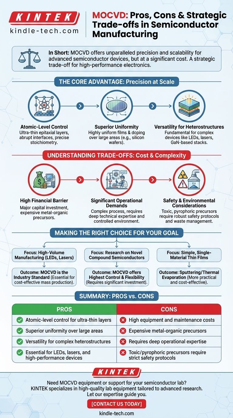
In short, MOCVD offers unparalleled precision and scalability for manufacturing advanced semiconductor devices, but at a significant cost. This technique, formally known as Metalorganic Chemical Vapor Deposition, allows for the growth of extremely pure, uniform crystalline layers. This control is critical for high-performance electronics, but it demands expensive equipment, costly materials, and deep operational expertise.
The core decision to use MOCVD is a strategic trade-off. You are choosing to accept high initial costs and operational complexity in exchange for unmatched control over material quality and the ability to scale production for complex devices like LEDs and lasers.

The Core Advantage: Precision at Scale
MOCVD is not merely a deposition technique; it is a foundational process for building the high-performance compound semiconductors that power modern technology. Its primary advantages lie in its ability to combine atomic-level control with the demands of large-scale manufacturing.
Atomic-Level Control of Film Growth
The process allows for the deposition of ultra-thin epitaxial layers, sometimes just a few atoms thick.
This enables the creation of abrupt interfaces between different material layers, which is crucial for the performance of advanced electronic and optoelectronic devices. Control over film stoichiometry, or the precise ratio of elements, is also far easier to manage compared to other methods.
Superior Doping and Composition Uniformity
A key strength of MOCVD is its ability to produce highly uniform films over large areas, such as an entire silicon wafer.
This includes precise control over doping, the intentional introduction of impurities to alter the material's electrical properties. This uniformity is essential for achieving high yields in mass production.
Versatility for Complex Heterostructures
MOCVD is exceptionally well-suited for growing heterostructures, which are structures composed of multiple, distinct material layers.
This capability is fundamental to manufacturing devices like high-brightness LEDs and semiconductor lasers, which rely on a sophisticated stack of carefully engineered layers, often using materials like Gallium Nitride (GaN).
Understanding the Trade-offs: Cost and Complexity
While powerful, MOCVD is not a universally applicable solution. Its adoption is limited by significant practical and financial challenges that must be carefully considered.
The High Financial Barrier to Entry
The most immediate disadvantage is cost. The equipment purchase, installation, and ongoing maintenance represent a major capital investment.
Furthermore, the metal-organic precursors used as the source materials are themselves very expensive, contributing significantly to the high operational costs.
Significant Operational Demands
MOCVD is often described as a "challenging art form" because it is a complex process to implement.
It requires a highly controlled lab environment and, more importantly, a team with deep technical expertise to dial in and maintain the process parameters for consistent, high-quality results.
Safety and Environmental Considerations
Many of the precursor gases and liquids used in MOCVD are toxic, pyrophoric (ignite spontaneously in air), or both.
This necessitates robust safety protocols, specialized handling equipment, and careful management of chemical waste, adding to both the complexity and environmental footprint of the operation.
Making the Right Choice for Your Goal
Selecting a deposition technology requires aligning its capabilities with your primary objective. MOCVD is a specialized tool designed for demanding applications.
- If your primary focus is high-volume manufacturing of complex optoelectronics (like LEDs and lasers): MOCVD is the undisputed industry standard, as its precision and scalability are essential for cost-effective mass production.
- If your primary focus is research on novel compound semiconductor devices: MOCVD offers the highest degree of control and flexibility, but you must be prepared for the significant investment in equipment and process expertise.
- If your primary focus is depositing simple, single-material thin films: The high overhead of MOCVD is unnecessary; more accessible techniques like sputtering or thermal evaporation are far more practical and cost-effective.
Ultimately, choosing MOCVD is an investment in manufacturing capability, enabling the production of advanced electronic devices that are otherwise unattainable.
Summary Table:
| Pros of MOCVD | Cons of MOCVD |
|---|---|
| Atomic-level control for ultra-thin layers | High equipment and maintenance costs |
| Superior uniformity over large areas | Expensive metal-organic precursors |
| Versatility for complex heterostructures | Requires deep operational expertise |
| Essential for LEDs, lasers, and high-performance devices | Toxic/pyrophoric precursors require strict safety protocols |
Need MOCVD equipment or support for your semiconductor lab? KINTEK specializes in providing high-quality lab equipment and consumables tailored to advanced research and production needs. Our expertise can help you navigate the complexities of MOCVD technology, ensuring you achieve optimal performance and efficiency. Contact us today to discuss how we can support your laboratory's goals!
Visual Guide
Related Products
- Multi Heating Zones CVD Tube Furnace Machine Chemical Vapor Deposition Chamber System Equipment
- 915MHz MPCVD Diamond Machine Microwave Plasma Chemical Vapor Deposition System Reactor
- Microwave Plasma Chemical Vapor Deposition MPCVD Machine System Reactor for Lab and Diamond Growth
- Cylindrical Resonator MPCVD Machine System Reactor for Microwave Plasma Chemical Vapor Deposition and Lab Diamond Growth
- Molybdenum Vacuum Heat Treat Furnace
People Also Ask
- What is the function of a high-temperature CVD tube furnace in 3D graphene foam prep? Master 3D Nanomaterial Growth
- What are the differences between chemical vapour deposition processes? A Guide to Pressure, Quality & Cost
- What is a CVD tube furnace? A Complete Guide to Thin-Film Deposition
- What is the function of a tube furnace in CVD SiC synthesis? Achieving Ultra-Pure Silicon Carbide Powders
- What advantages do CVD furnaces offer for Wf/W composites? Preserving Fiber Ductility and Interface Integrity