In semiconductor manufacturing, deposition techniques fall into two primary categories: Chemical Vapor Deposition (CVD) and Physical Vapor Deposition (PVD). These processes are used to apply thin films of various materials onto a silicon wafer, forming the intricate layers of insulating, conductive, and semiconducting materials that make up a modern integrated circuit. A third, highly precise method called Atomic Layer Deposition (ALD) is also critical for advanced chip designs.
The core challenge is not simply knowing the names of deposition techniques, but understanding why a specific method is chosen. The decision hinges on a fundamental trade-off between deposition speed, the quality of the film, and its ability to uniformly cover complex, microscopic 3D structures on the wafer.
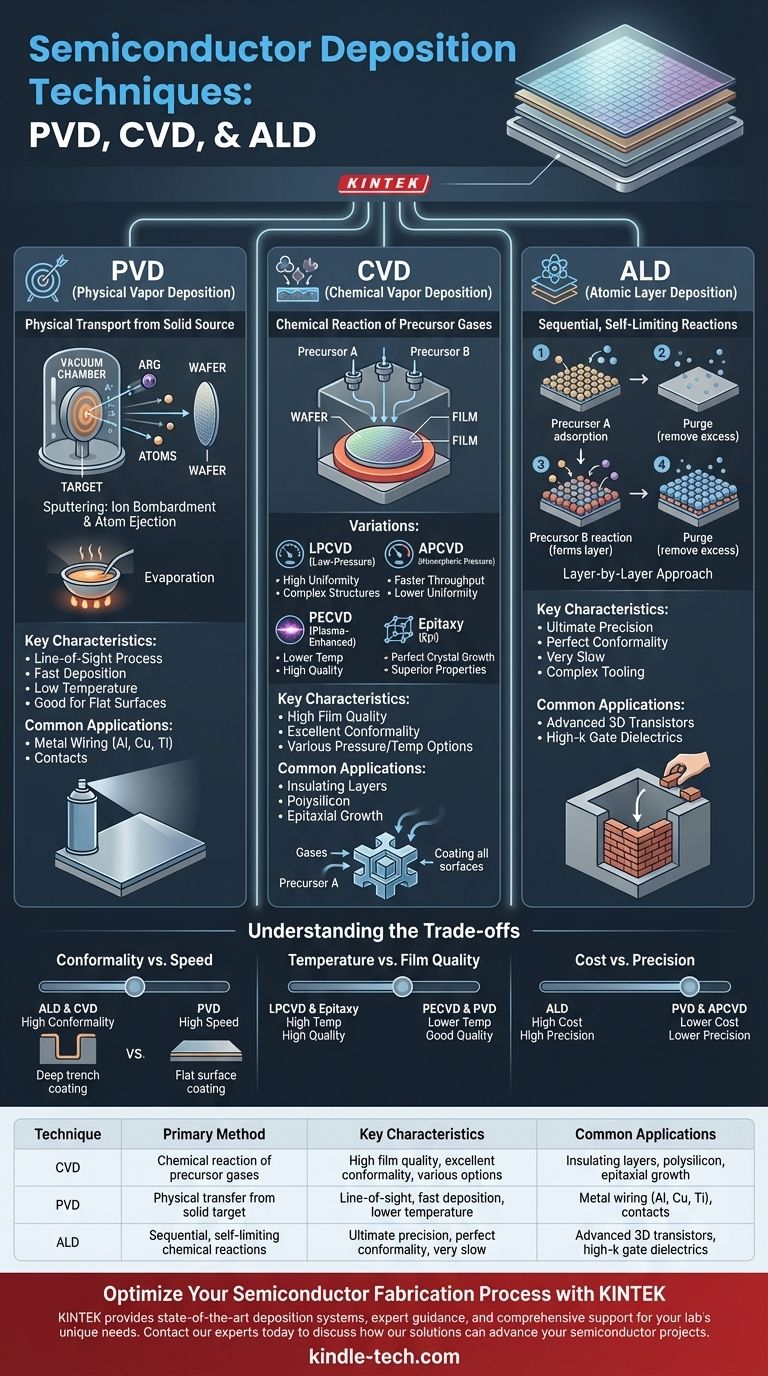
The Two Pillars of Deposition: PVD and CVD
At the highest level, deposition methods are distinguished by how they get material from a source to the wafer's surface. One uses a chemical reaction, while the other uses a physical process.
Chemical Vapor Deposition (CVD)
CVD is the most widely used deposition technology in the industry. It involves introducing one or more reactive gases, known as precursors, into a reaction chamber.
These gases react chemically near or on the hot wafer surface, forming a new, solid material that deposits as a thin film.
Physical Vapor Deposition (PVD)
PVD, in contrast, does not involve a chemical reaction to create the film material. Instead, it transports material from a solid source or target to the wafer using physical means.
This is typically done in a vacuum. Think of it as physically moving atoms from point A (the source) to point B (the wafer).
Diving Deep into Chemical Vapor Deposition (CVD)
Because CVD relies on chemical reactions, it can produce very high-quality, pure, and uniform films. The specific conditions of the reaction lead to several variations of CVD, each with a different purpose.
The Role of Pressure and Plasma
Low-Pressure CVD (LPCVD): By operating at very low pressures, LPCVD allows gas molecules to move more freely, resulting in highly uniform films that can coat complex structures evenly. It is often used for high-quality insulation and polysilicon layers.
Atmospheric Pressure CVD (APCVD): This method operates at normal atmospheric pressure, making it a faster and higher-throughput process. However, the film quality and uniformity are generally lower than LPCVD.
Plasma-Enhanced CVD (PECVD): This technique uses an electrical plasma to give energy to the precursor gases. This added energy allows the chemical reaction to occur at much lower temperatures, which is crucial for preventing damage to sensitive structures already built on the wafer.
The Special Case of Epitaxy
Epitaxial Deposition (Epi): This is a highly specialized form of CVD used to grow a single-crystal silicon layer on top of a single-crystal silicon wafer. The new layer perfectly mimics the crystal structure of the substrate, resulting in a flawless film with superior electronic properties.
Understanding Physical Vapor Deposition (PVD)
PVD is fundamentally a line-of-sight process, making it excellent for depositing films on flat surfaces quickly. The most common PVD technique in semiconductor manufacturing is sputtering.
Sputtering Explained
In sputtering, a target made of the desired deposition material is bombarded with high-energy ions (usually Argon) inside a vacuum chamber.
This bombardment physically knocks atoms off the target, which then travel and deposit onto the wafer. It is a highly versatile method used for depositing metals like aluminum, copper, and titanium for wiring.
Other PVD Methods
Another PVD technique is evaporation, where a source material is heated in a vacuum until it evaporates. The gaseous atoms then travel to the wafer and condense, forming a film. While less common for advanced logic chips, it is still used in other areas of electronics manufacturing.
The Rise of Atomic Layer Deposition (ALD)
For the most advanced chips with microscopic, three-dimensional transistors, a technique with ultimate precision is required. This is where Atomic Layer Deposition (ALD) comes in.
A Layer-by-Layer Approach
ALD is a subtype of CVD that breaks the deposition process into sequential, self-limiting steps. It exposes the wafer to one precursor gas, which forms exactly one atomic layer, and then purges the chamber. It then introduces a second precursor to react with the first layer, completing the film one atomic layer at a time.
Why ALD is Critical
While extremely slow, ALD provides unparalleled control over film thickness and conformality—the ability to deposit a perfectly uniform film over incredibly complex and deep trench-like structures. This is non-negotiable for modern FinFET transistors and advanced memory devices.
Understanding the Trade-offs
Choosing a deposition technology requires balancing competing priorities.
Conformality vs. Speed
CVD and especially ALD excel at conformality. Because the precursor gases can reach all parts of a complex surface, the resulting film is highly uniform.
PVD is a line-of-sight technique. Like a spray-paint can, it covers what it can "see," making it difficult to coat the bottom and sidewalls of deep trenches evenly. However, PVD is generally much faster than ALD.
Temperature vs. Film Quality
High-temperature processes like LPCVD often produce very high-quality films. However, high temperatures can damage or alter previously deposited layers.
PECVD is the solution here, using plasma to enable high-quality deposition at lower temperatures. PVD can also be a low-temperature process.
Cost vs. Precision
Simpler, faster processes like APCVD or PVD are less expensive to run. ALD, with its slow, multi-step nature and complex tooling, is the most expensive but offers a level of precision that is simply unattainable with other methods.
Choosing the Right Deposition Strategy
Your choice of technology is dictated entirely by the requirements of the specific film layer you are creating.
- If your primary focus is bulk metal wiring on a relatively flat surface: PVD (sputtering) is the efficient and cost-effective choice.
- If your primary focus is a high-quality insulating film over gentle topography: A standard CVD method like LPCVD or PECVD provides the right balance of quality and throughput.
- If your primary focus is creating a flawless film on the gate of a cutting-edge 3D transistor: ALD is the only option that provides the required precision and conformality, despite its cost and slow speed.
Ultimately, understanding the fundamental principles of each technique empowers you to select the right tool for the right job in the complex world of semiconductor fabrication.
Summary Table:
| Technique | Primary Method | Key Characteristics | Common Applications |
|---|---|---|---|
| CVD (Chemical Vapor Deposition) | Chemical reaction of precursor gases | High film quality, excellent conformality, various pressure/temperature options | Insulating layers, polysilicon, epitaxial growth |
| PVD (Physical Vapor Deposition) | Physical transfer from solid target | Line-of-sight, fast deposition, lower temperature | Metal wiring (Al, Cu, Ti), contacts |
| ALD (Atomic Layer Deposition) | Sequential, self-limiting chemical reactions | Ultimate precision, perfect conformality, very slow | Advanced 3D transistors, high-k gate dielectrics |
Optimize Your Semiconductor Fabrication Process with KINTEK
Choosing the right deposition technique is critical for achieving the perfect balance of film quality, conformality, and throughput in your semiconductor manufacturing. Whether you require the high-speed capabilities of PVD, the excellent conformality of CVD, or the atomic-level precision of ALD, KINTEK has the expertise and equipment to support your lab's unique needs.
As a specialist in advanced lab equipment and consumables, KINTEK provides:
- State-of-the-art deposition systems tailored to your research and production requirements
- Expert guidance on selecting the optimal technique for your specific applications
- Comprehensive support for semiconductor laboratories developing next-generation chips
Ready to enhance your deposition capabilities? Contact our experts today to discuss how KINTEK's solutions can advance your semiconductor fabrication projects.
Visual Guide
Related Products
- RF PECVD System Radio Frequency Plasma-Enhanced Chemical Vapor Deposition RF PECVD
- Chemical Vapor Deposition CVD Equipment System Chamber Slide PECVD Tube Furnace with Liquid Gasifier PECVD Machine
- CVD Diamond for Thermal Management Applications
- Electron Beam Evaporation Coating Oxygen-Free Copper Crucible and Evaporation Boat
- 915MHz MPCVD Diamond Machine Microwave Plasma Chemical Vapor Deposition System Reactor
People Also Ask
- Why is a Matching Network Indispensable in RF-PECVD for Siloxane Films? Ensure Stable Plasma and Uniform Deposition
- What is plasma enhanced chemical vapour deposition PECVD used for? Enable Low-Temp Thin Films for Electronics & Solar
- What is plasma enhanced chemical Vapour deposition process used for fabrication of? A Guide to Low-Temperature Thin Films
- What is plasma enhanced chemical vapour deposition process? Unlock Low-Temperature, High-Quality Thin Films
- What is plasma CVD? Unlock Low-Temperature Thin Film Deposition for Sensitive Materials