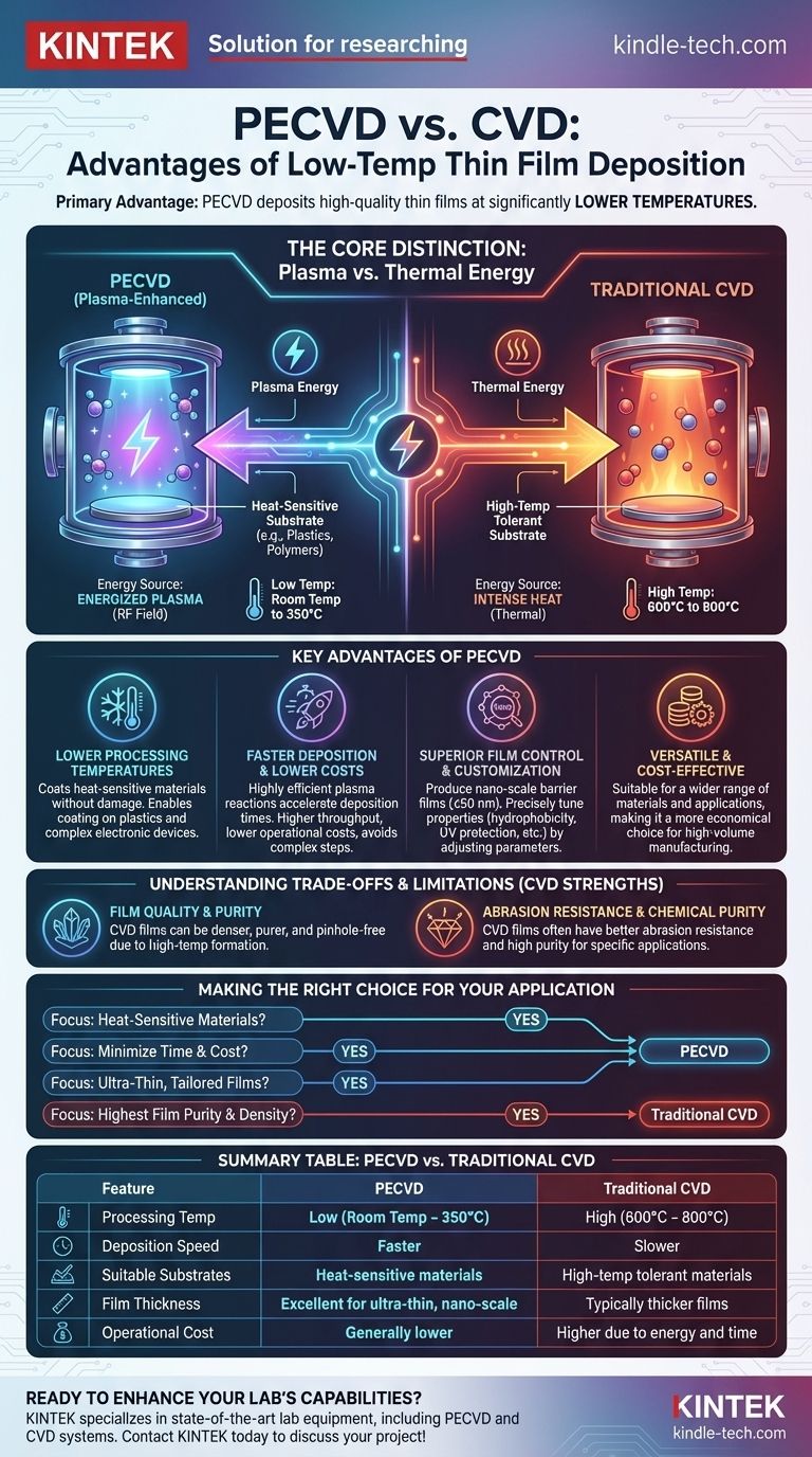
The primary advantage of Plasma-Enhanced Chemical Vapor Deposition (PECVD) over traditional Chemical Vapor Deposition (CVD) is its ability to deposit high-quality thin films at significantly lower temperatures. This fundamental difference, along with faster deposition rates, makes PECVD a more versatile and cost-effective solution for a wider range of materials, especially those sensitive to heat.
The core distinction is not simply about which method is "better," but how each one supplies energy. Traditional CVD uses high heat to drive chemical reactions, while PECVD uses an energized gas, or plasma, to achieve the same result at or near room temperature. This single difference in energy source dictates the process speed, cost, and suitable applications for each technology.
The Core Distinction: Plasma vs. Thermal Energy
To understand the advantages of PECVD, we must first understand the fundamental mechanism that separates it from traditional CVD. Both processes aim to deposit a solid thin film from gaseous precursors inside a vacuum chamber. The key difference is how they provide the activation energy required for this transformation.
How Heat Drives CVD
Traditional CVD relies on thermal energy. The substrate is heated to very high temperatures, typically between 600°C and 800°C.
This intense heat provides the energy needed to break the chemical bonds of the precursor gases, allowing them to react and deposit onto the substrate surface. This is a simple but energy-intensive approach.
How Plasma Drives PECVD
PECVD uses plasma as its energy source. Instead of heating the entire chamber, an electric field (typically radio frequency) is applied to the precursor gas, stripping electrons from the atoms and creating a highly reactive, ionized gas known as plasma.
This energized plasma provides the activation energy for the chemical reactions, allowing the deposition to occur at much lower temperatures, often from room temperature up to 350°C.
Key Advantages of PECVD Explained
This fundamental shift from thermal energy to plasma energy creates several significant operational advantages for PECVD.
Lower Processing Temperatures
This is the most critical advantage. The ability to deposit films without high heat means PECVD can coat temperature-sensitive substrates like plastics, polymers, and complex electronic devices that would be damaged or destroyed by traditional CVD temperatures.
Faster Deposition and Lower Costs
The reactions within a plasma are highly efficient and accelerated by the RF field, leading to significantly faster deposition times compared to the slow, heat-driven CVD process, which can take many hours.
Faster cycle times directly translate to higher throughput and lower operational costs. Furthermore, PECVD often avoids the expensive and time-consuming masking and de-masking steps required in many CVD processes.
Superior Film Control and Customization
PECVD provides excellent control over the properties of the deposited film. It can produce extremely thin, "nano-scale" barrier films (50 nm or less) with low internal stress.
By adjusting the gas mixture, pressure, and plasma power, engineers can precisely tune film characteristics such as hydrophobicity, UV protection, and oxygen resistance.
Understanding the Trade-offs and Limitations
While powerful, PECVD is not universally superior. Choosing the right method requires understanding its limitations, which often represent the strengths of traditional CVD.
Film Quality and Barrier Properties
While CVD films are thick, their high-temperature formation process can result in highly pure, dense, and pinhole-free films with excellent integrity.
In contrast, PECVD films can sometimes have weaker barrier properties and may be softer or less durable, though this is highly dependent on the specific process parameters used.
Abrasion Resistance
Due to the softer materials often deposited at lower temperatures, PECVD coatings can have limited abrasion resistance. While rework is possible, the films can be more susceptible to handling issues.
Chemical Purity
The high-heat environment of CVD is excellent for producing very high-purity single- or polycrystalline films. The plasma environment of PECVD can sometimes introduce impurities or result in amorphous film structures, which may not be suitable for all applications.
Making the Right Choice for Your Application
The decision between PECVD and CVD should be driven entirely by your substrate, desired film properties, and production goals.
- If your primary focus is coating heat-sensitive materials: PECVD is the only viable choice due to its low-temperature processing.
- If your primary focus is achieving the highest possible film purity or density: Traditional CVD may be superior, provided your substrate can tolerate the extreme heat.
- If your primary focus is minimizing production time and cost: PECVD's faster deposition rates and simpler workflow make it the more economical option for high-volume manufacturing.
- If your primary focus is creating ultra-thin films with tailored properties: PECVD offers the necessary control for nano-scale and highly customized coatings.
Ultimately, understanding the core difference between thermal and plasma energy empowers you to select the ideal deposition strategy for your specific technical and business goals.
Summary Table:
| Feature | PECVD | Traditional CVD |
|---|---|---|
| Processing Temperature | Low (Room Temp - 350°C) | High (600°C - 800°C) |
| Deposition Speed | Faster | Slower |
| Suitable Substrates | Heat-sensitive materials (plastics, polymers) | High-temperature tolerant materials |
| Film Thickness | Excellent for ultra-thin, nano-scale films | Typically thicker films |
| Operational Cost | Generally lower | Higher due to energy and time |
Ready to Enhance Your Lab's Capabilities with Advanced Thin Film Deposition?
Choosing the right deposition technology is critical for your research and production success. KINTEK specializes in providing state-of-the-art lab equipment, including PECVD and CVD systems, to meet your specific material science and coating needs.
We help you:
- Protect heat-sensitive substrates with low-temperature PECVD processes.
- Increase throughput and reduce costs with faster deposition rates.
- Achieve precise film properties tailored to your application requirements.
Let our experts guide you to the optimal solution for your laboratory. Contact KINTEK today to discuss your project and discover how our expertise in lab equipment can drive your innovation forward!
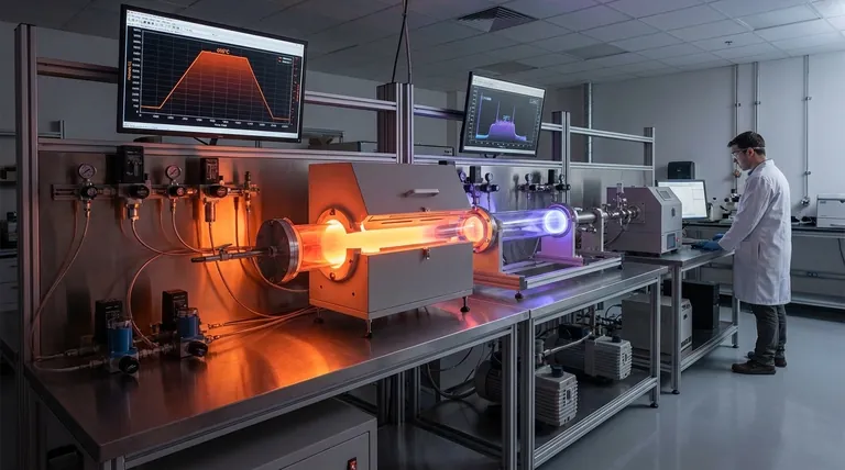
Visual Guide
Related Products
- Inclined Rotary Plasma Enhanced Chemical Vapor Deposition PECVD Equipment Tube Furnace Machine
- Chemical Vapor Deposition CVD Equipment System Chamber Slide PECVD Tube Furnace with Liquid Gasifier PECVD Machine
- Inclined Rotary Plasma Enhanced Chemical Vapor Deposition PECVD Equipment Tube Furnace Machine
- RF PECVD System Radio Frequency Plasma-Enhanced Chemical Vapor Deposition RF PECVD
- Multi Heating Zones CVD Tube Furnace Machine Chemical Vapor Deposition Chamber System Equipment
People Also Ask
- What are the benefits of plasma enhanced CVD? Achieve High-Quality, Low-Temperature Film Deposition
- How does plasma enhanced chemical vapor deposition work? Enable Low-Temperature Thin Film Deposition
- How does PECVD equipment facilitate the directional growth of carbon nanotubes? Achieve Precision Vertical Alignment
- What is plasma enhanced chemical vapour deposition PECVD used for? Enable Low-Temp Thin Films for Electronics & Solar
- Why is a PECVD system required for vertical graphene synthesis? Master Directional Control for 3D Nanostructures


