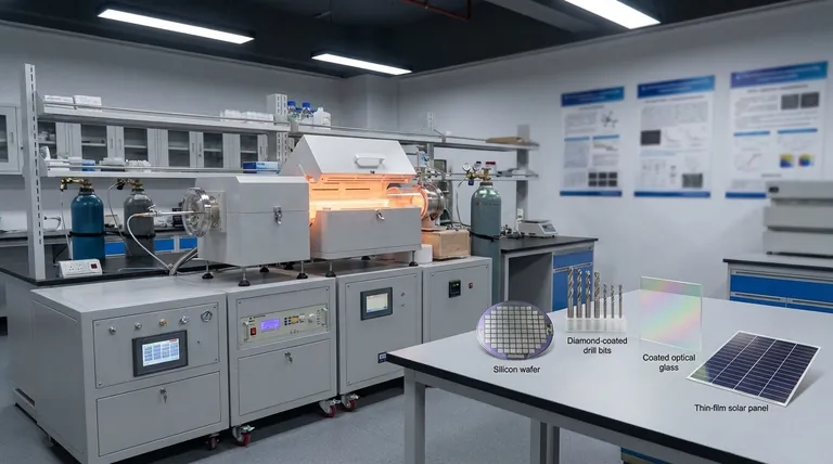
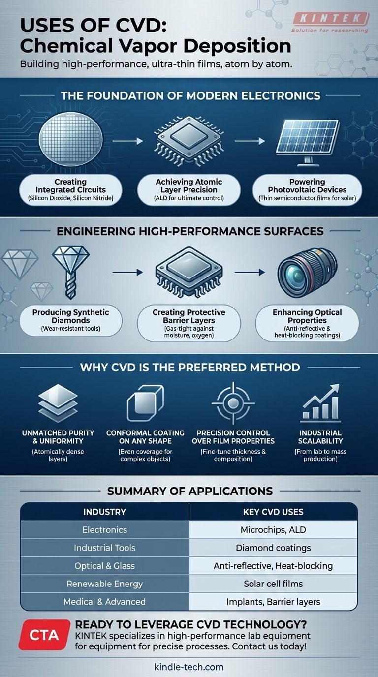
At its core, Chemical Vapor Deposition (CVD) is a sophisticated process for building high-performance, ultra-thin films of material onto a surface, atom by atom. Its uses span a vast range of industries, from fabricating the microchips in your phone and computer to creating incredibly durable, wear-resistant coatings for industrial tools and enhancing the properties of glass. It is also used to produce synthetic diamonds and advanced materials for solar panels and medical implants.
The true power of CVD isn't just what it's used for, but why it's indispensable. Its unique ability to create exceptionally pure, dense, and perfectly uniform coatings on even the most complex shapes makes it a foundational technology for modern manufacturing where precision is paramount.
The Foundation of Modern Electronics
The semiconductor industry relies heavily on CVD to build the microscopic structures that power all modern electronic devices. The process is essential for creating the layered, intricate architecture of an integrated circuit.
Creating Integrated Circuits
Every computer chip is composed of millions or billions of transistors, built by depositing extremely thin layers of different materials onto a silicon wafer. CVD is the primary method used to lay down these critical films, such as silicon dioxide (an insulator) and silicon nitride (a protective layer).
The process ensures these layers are deposited with exceptional purity and uniformity, which is non-negotiable for chip performance and reliability.
Achieving Atomic Layer Precision
As electronic components continue to shrink, the precision required to manufacture them grows exponentially. Advanced forms of CVD, like Atomic Layer Deposition (ALD), allow engineers to build films one single atomic layer at a time, offering the ultimate control over thickness and composition.
Powering Photovoltaic Devices
The same principles that apply to computer chips are also used to create solar cells. CVD is used to deposit the thin semiconductor films that are responsible for converting sunlight into electricity, making it a key process in the renewable energy sector.
Engineering High-Performance Surfaces
Beyond electronics, CVD is a dominant technique for fundamentally changing the surface properties of a material, making it stronger, more resilient, or giving it new chemical characteristics.
Producing Synthetic Diamonds
CVD can be used to grow layers of synthetic diamond—one of the hardest materials known—on other surfaces. This is commonly applied to industrial cutting tools, drill bits, and other components, dramatically increasing their lifespan and performance by making them incredibly wear-resistant.
Creating Protective Barrier Layers
Many products require protection from the environment. CVD is used to deposit dense, non-porous films that act as gas-tight barriers against moisture, oxygen, and other corrosive elements.
This is critical for applications like protecting sensitive electronic components, creating anti-tarnish coatings, and even lining food packaging.
Enhancing Optical Properties
CVD is used to apply microscopically thin coatings to glass and plastics to control how they interact with light. This includes creating anti-reflective coatings on camera lenses and eyeglasses or depositing heat-blocking layers on architectural glass to improve energy efficiency.
Why CVD is the Preferred Method
The widespread adoption of CVD stems from several core advantages that alternative coating techniques cannot easily match. These capabilities directly enable its diverse applications.
Unmatched Purity and Uniformity
Because CVD is a chemical process that builds a film from gaseous precursors, the resulting layers are extremely pure and dense. This is a stark contrast to mechanical methods and is essential for the electrical properties of semiconductors.
Conformal Coating on Any Shape
Unlike line-of-sight deposition methods (like sputtering), the gases in a CVD process can flow around and coat all surfaces of a complex, three-dimensional object evenly. This ability to create a conformal coating is vital for components with intricate or irregular shapes.
Precision Control Over Film Properties
Engineers have precise control over the CVD process, allowing them to fine-tune the thickness, composition, and microstructure of the film. This means they can engineer surfaces with very specific properties, whether it's electrical conductivity, hardness, or a certain refractive index.
Industrial Scalability
CVD processes are highly scalable, working effectively for everything from small-scale laboratory research to the large-scale industrial production required for manufacturing millions of computer chips or coating vast sheets of architectural glass.
Matching the Method to Your Goal
The right application of CVD depends entirely on the desired outcome. Understanding your primary objective is key to leveraging its power.
- If your primary focus is microelectronics: The key is CVD's ability to deposit ultra-pure, atomically precise, and perfectly uniform films on silicon wafers.
- If your primary focus is mechanical durability: The takeaway is its power to create exceptionally hard, wear-resistant ceramic and diamond coatings for tools and components.
- If your primary focus is advanced materials: The value lies in its versatility to engineer surfaces with unique optical, chemical barrier, or filtration properties.
Ultimately, Chemical Vapor Deposition is the go-to technology for building superior materials from the ground up, enabling innovation across nearly every advanced industry.
Summary Table:
| Industry/Application | Key CVD Uses |
|---|---|
| Electronics | Fabricating microchips, depositing insulating layers (e.g., silicon dioxide), Atomic Layer Deposition (ALD) |
| Industrial Tools | Creating wear-resistant diamond coatings for cutting tools and drill bits |
| Optical & Glass | Applying anti-reflective and heat-blocking coatings on lenses and architectural glass |
| Renewable Energy | Depositing thin semiconductor films for solar cells |
| Medical & Advanced Materials | Producing synthetic diamonds, medical implants, and protective barrier layers |
| Key Advantages | Exceptional purity, uniform/conformal coatings, precision control, scalability |
Ready to leverage CVD technology for your lab's advanced material needs?
At KINTEK, we specialize in providing high-performance lab equipment and consumables tailored for precise Chemical Vapor Deposition processes. Whether you're developing microelectronics, durable coatings, or innovative materials, our solutions ensure purity, uniformity, and scalability.
Contact us today to discuss how our CVD expertise can enhance your research and production outcomes!
Visual Guide
Related Products
- CVD Diamond Dressing Tools for Precision Applications
- Multi Heating Zones CVD Tube Furnace Machine Chemical Vapor Deposition Chamber System Equipment
- CVD Diamond Domes for Industrial and Scientific Applications
- CVD Diamond for Thermal Management Applications
- Chemical Vapor Deposition CVD Equipment System Chamber Slide PECVD Tube Furnace with Liquid Gasifier PECVD Machine
People Also Ask
- How do you identify a CVD diamond? The Definitive Guide to Lab-Grown Diamond Verification
- Can CVD diamonds change color? No, their color is permanent and stable.
- What color diamonds are CVD? Understanding the Process from Brown Tint to Colorless Beauty
- Does the chemical vapor deposition be used for diamonds? Yes, for Growing High-Purity Lab Diamonds
- How long does it take to make synthetic diamonds? Discover the 6-8 Week Science Behind Lab-Grown Gems


