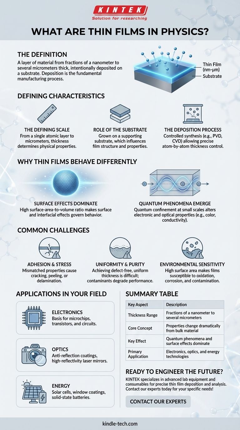
In physics, a thin film is a layer of material with a thickness ranging from fractions of a nanometer to several micrometers. These layers are intentionally created on the surface of a solid support, known as a substrate. The controlled process of creating these films is called deposition, and it is fundamental to manufacturing many modern technologies.
The critical concept to grasp is that a material's properties can change dramatically when it is made into a thin film. By controlling thickness at the atomic level, we can unlock unique electronic, optical, and magnetic behaviors that are not present in the material's bulk form.
What Qualifies as a "Thin" Film?
A thin film is defined by more than just its physical size. Its identity is tied to its relationship with a substrate and the unique physical phenomena that emerge at such a small scale.
The Defining Scale
A thin film's thickness can be as small as a single layer of atoms (a few angstroms) or as large as several micrometers (millionths of a meter). This range is where the film's thickness becomes a dominant factor in its overall physical properties.
The Role of the Substrate
Thin films do not exist in isolation. They are grown or deposited onto a supporting material called a substrate. The substrate provides the mechanical foundation for the film, and its interaction with the film can influence the film's crystal structure and properties.
The Deposition Process
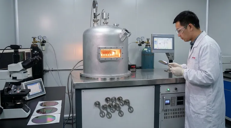
The creation of a thin film is a highly controlled synthesis process. Techniques like physical vapor deposition (PVD) or chemical vapor deposition (CVD) are used to deposit material atom by atom or molecule by molecule onto the substrate, allowing for precise control over thickness and structure.
Why Thin Films Behave Differently
The reason thin films are so crucial in science and engineering is that their properties diverge significantly from the same material in bulk form. This divergence is driven by effects that are negligible in larger objects.
The Dominance of Surface Effects
In a thin film, a huge proportion of its atoms are at a surface or interface. This massive surface-area-to-volume ratio means that surface energy and interfacial effects, which are minor in a bulk material, become dominant forces that govern the film's behavior.
Emergence of Quantum Phenomena
When a film's thickness approaches the de Broglie wavelength of electrons within the material, quantum confinement occurs. This restricts the energy levels of electrons, fundamentally changing the material's electronic and optical properties, such as its color or electrical conductivity.
Engineering Unique Properties
Because of these effects, scientists and engineers can tune a material's properties by precisely controlling the film's thickness, crystal structure, and composition. This allows for the creation of materials with tailored characteristics for specific applications, as mentioned in the references.
Common Challenges and Considerations
Working with thin films involves a unique set of engineering challenges that are critical to overcome for any practical application.
Adhesion and Internal Stress
Ensuring the film adheres properly to the substrate is paramount. Mismatches in the material properties between the film and substrate can create immense internal stress, causing the film to crack, peel, or delaminate.
Uniformity and Purity
Achieving a perfectly uniform thickness and a pure, defect-free structure across the entire substrate is extremely difficult. Contaminants or variations in the deposition process can create imperfections that degrade the film's performance.
Environmental Sensitivity
The high surface area that gives thin films their unique properties also makes them highly susceptible to their environment. Oxidation, corrosion, and contamination can easily alter or destroy the film's functionality if it is not properly protected.
How This Applies to Your Field
The application of thin film physics is vast and is a cornerstone of nearly all modern technology. Your interest in them likely connects to one of these major areas.
- If your primary focus is electronics: Thin films are the basis for all microchips, where layers of semiconducting, insulating, and conducting films create transistors and circuits.
- If your primary focus is optics: Thin film coatings are used to create anti-reflection layers on glasses and camera lenses, as well as highly reflective mirrors for lasers.
- If your primary focus is energy: Thin films are essential for modern solar cells, energy-efficient window coatings, and solid-state batteries.
Ultimately, mastering the principles of thin films is to understand how we manipulate matter at its most fundamental levels to engineer the tools of the future.
Summary Table:
| Key Aspect | Description |
|---|---|
| Thickness Range | Fractions of a nanometer to several micrometers |
| Core Concept | Properties change dramatically from bulk material |
| Key Effect | Quantum phenomena and surface effects dominate |
| Primary Application | Electronics, optics, and energy technologies |
Ready to Engineer the Future with Thin Films?
KINTEK specializes in the advanced lab equipment and consumables required for precise thin film deposition and analysis. Whether you are developing next-generation microchips, optical coatings, or solar cells, our solutions provide the control and reliability needed to master material properties at the nanoscale.
Let us help you unlock the potential of thin films in your research or production. Contact our experts today to discuss your specific laboratory needs!
Visual Guide