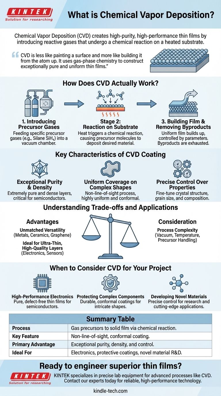
In essence, Chemical Vapor Deposition (CVD) is a process used to create high-purity, high-performance thin films on a surface. It works by introducing reactive gases (precursors) into a chamber, where they undergo a chemical reaction on a heated substrate, leaving behind a solid layer of the desired material. This method allows for the construction of materials layer by layer, offering exceptional control over thickness, purity, and structure.
Chemical Vapor Deposition is less like painting a surface and more like building it from the atom up. It uses gas-phase chemistry to construct exceptionally pure and uniform thin films, making it a cornerstone technology for manufacturing high-performance electronics and advanced materials.
How Does CVD Actually Work?
At its core, CVD is a carefully controlled chemical reaction that transforms gases into a solid. The process can be broken down into a few fundamental stages.
Stage 1: Introducing the Reactant Gases
The process begins by feeding specific gases, known as precursors, into a reaction chamber that is typically under vacuum. These precursors contain the chemical elements needed for the final film.
For example, to deposit a film of pure silicon, a gas like silane (SiH₄) might be used as the precursor.
Stage 2: The Reaction on the Substrate
Inside the chamber, a base material, called the substrate, is heated to a precise temperature. When the precursor gases flow over this hot surface, the heat provides the energy needed to trigger a chemical reaction.
This reaction causes the precursor molecules to break apart, "depositing" the desired solid material directly onto the substrate surface.
Stage 3: Building the Film and Removing Byproducts
The solid material builds up on the substrate, forming a thin, uniform film. The thickness of this film is controlled with incredible precision by adjusting process parameters like time, temperature, and gas flow.
Any unwanted chemical elements from the reaction form gaseous byproducts. These are harmlessly swept out of the chamber, leaving behind an exceptionally pure final coating.
Key Characteristics of a CVD Coating
The reason CVD is so widely used is because of the superior qualities of the films it produces. It isn't just a coating; it's an engineered layer.
Exceptional Purity and Density
Because the process builds the film from purified gas precursors in a controlled environment, the resulting layers are extremely pure and dense. This is critical for applications like semiconductors, where even tiny impurities can ruin device performance.
Uniform Coverage on Complex Shapes
CVD is a non-line-of-sight process. The gas flows around the entire substrate, no matter how complex its shape. This results in a highly uniform, or conformal, coating that perfectly wraps around every feature of the component.
Precise Control Over Material Properties
By carefully adjusting the deposition parameters—such as temperature, pressure, and gas composition—engineers can fine-tune the final material. They can control the crystal structure, grain size, and even chemical composition, tailoring the film for a specific purpose.
Understanding the Trade-offs and Applications
CVD is a powerful but specialized tool. Choosing it requires understanding its primary advantages and inherent complexities.
Advantage: Unmatched Versatility
The process is fundamentally based on chemical reactions, which gives it enormous versatility. CVD can be used to deposit a vast range of materials, including metals, ceramics, alloys, and advanced compounds like graphene.
Advantage: Ideal for Ultra-Thin, High-Quality Layers
CVD excels at creating films that are both ultra-thin and structurally perfect. This makes it the leading method for manufacturing high-performance electronics, sensors, and optical components where quality at the nanoscale is paramount.
Consideration: Process Complexity
The primary trade-off is the complexity of the equipment and process. CVD requires a vacuum chamber, precise temperature control, and careful handling of volatile precursor gases. This makes it more suitable for high-value applications where performance justifies the investment.
When to Consider CVD for Your Project
CVD is the right choice when the quality and performance of a surface layer are non-negotiable.
- If your primary focus is high-performance electronics: CVD is the industry standard for creating the pure, defect-free thin films required for semiconductors and advanced sensors.
- If your primary focus is protecting complex components: The conformal nature of CVD makes it ideal for applying durable, low-friction, or thermally resistant coatings to parts with intricate shapes.
- If your primary focus is developing novel materials: CVD offers the precise control needed to engineer materials with specific crystalline structures and properties for research and cutting-edge applications.
Ultimately, Chemical Vapor Deposition empowers engineers to build superior materials from the ground up, enabling the next generation of advanced technology.
Summary Table:
| Key Aspect | Description |
|---|---|
| Process | A chemical reaction transforms gas precursors into a solid film on a heated substrate. |
| Key Feature | Non-line-of-sight, conformal coating for complex shapes. |
| Primary Advantage | Exceptional purity, density, and precise control over film properties. |
| Ideal For | High-performance electronics, protective coatings, and novel material R&D. |
Ready to engineer superior thin films for your lab's projects?
KINTEK specializes in providing the precise lab equipment and consumables needed for advanced processes like Chemical Vapor Deposition. Whether you are developing next-generation semiconductors, applying protective coatings, or conducting cutting-edge materials research, our solutions are designed to meet the demanding requirements of your laboratory.
Contact our experts today to discuss how we can support your high-value applications with reliable, high-performance technology.
Visual Guide
Related Products
- Chemical Vapor Deposition CVD Equipment System Chamber Slide PECVD Tube Furnace with Liquid Gasifier PECVD Machine
- RF PECVD System Radio Frequency Plasma-Enhanced Chemical Vapor Deposition RF PECVD
- Microwave Plasma Chemical Vapor Deposition MPCVD Machine System Reactor for Lab and Diamond Growth
- Customer Made Versatile CVD Tube Furnace Chemical Vapor Deposition Chamber System Equipment
- 915MHz MPCVD Diamond Machine Microwave Plasma Chemical Vapor Deposition System Reactor
People Also Ask
- What are the core advantages of PE-CVD in OLED encapsulation? Protect Sensitive Layers with Low-Temp Film Deposition
- What types of substrates are used in CVD to facilitate graphene films? Optimize Graphene Growth with the Right Catalyst
- What happens during deposition chemistry? Building Thin Films from Gaseous Precursors
- Why is Chemical Vapor Deposition (CVD) equipment uniquely suited for constructing hierarchical superhydrophobic structures?
- What are the advantages of chemical vapor deposition? Achieve Superior Thin Films for Your Lab


