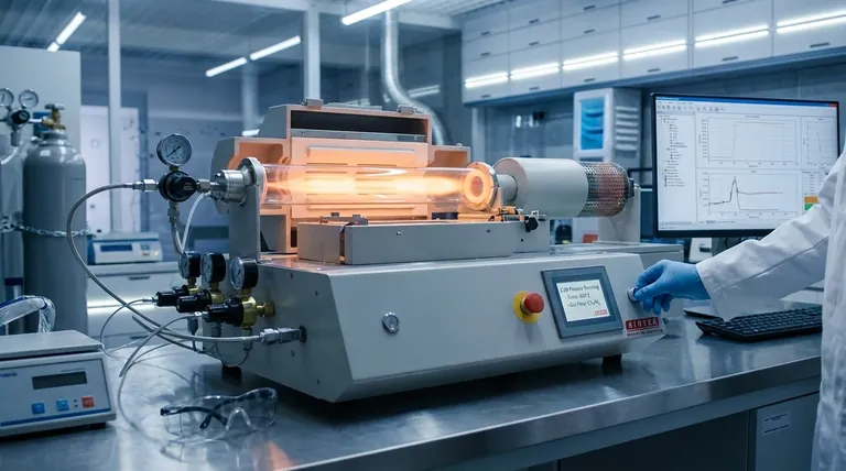
In essence, Chemical Vapor Deposition (CVD) is a sophisticated process for growing high-quality diamonds above ground. It works by placing a small diamond "seed" crystal inside a vacuum chamber, heating it to high temperatures, and introducing a carbon-rich gas like methane. The gas is energized into a plasma, which breaks it down and allows pure carbon atoms to attach to the seed, building a new diamond one atomic layer at a time.
The core insight is that CVD treats diamond not as a mineral to be mined, but as an advanced material to be engineered. This method offers precise control over the diamond's growth and properties, unlocking applications far beyond traditional jewelry.
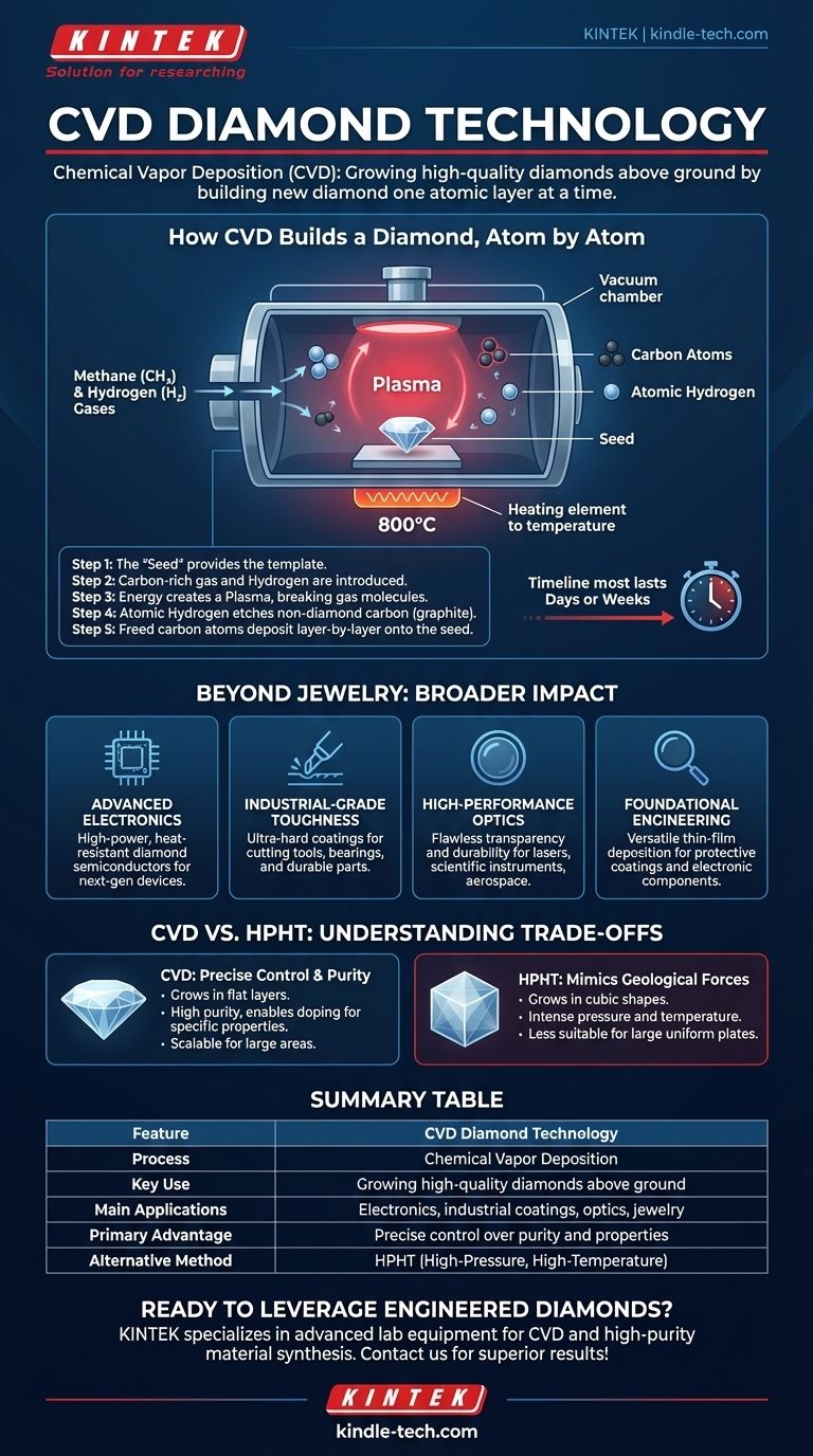
How CVD Builds a Diamond, Atom by Atom
The CVD process is a meticulously controlled sequence that mimics certain cosmic conditions, but in a laboratory setting. Each step is critical to forming a pure diamond crystal instead of a less-structured material like graphite.
The "Seed" and the Chamber
The process begins with a very thin, high-quality slice of an existing diamond, known as a seed. This seed provides the crystal lattice template for the new diamond to grow upon. It is placed inside a sealed, low-pressure vacuum chamber.
Introducing the Carbon Source
The chamber is filled with a carefully controlled mixture of gases, primarily a carbon source like methane (CH₄) and an abundance of hydrogen (H₂). These gases are the raw building blocks for the new diamond.
Creating the Plasma
The chamber is heated to around 800° Celsius, and energy, often from microwaves, is introduced. This energizes the gas mixture into a glowing ball of plasma, a state of matter where gas molecules are broken apart into their atomic components.
The Critical Role of Hydrogen
Within the plasma, atomic hydrogen serves as a "purifier." It bonds to and etches away any non-diamond carbon (graphite) that tries to form, but leaves the stronger diamond bonds untouched. This ensures that only a pure, defect-free diamond crystal structure can grow.
Layer-by-Layer Growth
The freed carbon atoms from the methane rain down onto the diamond seed. Because the seed's lattice is the most stable surface available, the carbon atoms lock into place, extending the crystal structure. This slow, methodical process continues for days or weeks, growing the diamond atom by atom.
Beyond Jewelry: The Broader Impact of CVD
While gem-quality diamonds are a prominent application, the underlying CVD technology is a foundational manufacturing process used across numerous high-tech industries.
A Foundational Engineering Process
CVD is a versatile technology for depositing thin, solid films of various inorganic materials. It's used to create everything from protective coatings to essential electronic components.
Applications in Advanced Electronics
The ability to produce pure, large-area diamond wafers makes CVD critical for creating next-generation semiconductors. These diamond-based components can handle higher power and heat than silicon, enabling more powerful and efficient electronics.
Industrial-Grade Toughness
CVD is used to apply ultra-hard diamond coatings to cutting tools, bearings, and other industrial parts. This dramatically increases their durability, wear resistance, and lifespan in demanding environments.
High-Performance Optics
Because CVD diamonds can be grown with flawless transparency and are incredibly durable, they are used to create lenses and windows for lasers, scientific instruments, and aerospace applications that must withstand extreme conditions.
Understanding the Trade-offs
CVD is not the only method for creating diamonds, and its advantages are best understood in context. The primary alternative is HPHT (High-Pressure, High-Temperature), which mimics the geological forces that form diamonds deep within the Earth.
Purity and Control
CVD's primary advantage is control. Because it is an atom-by-atom process, it allows for exceptional purity. It also enables scientists to intentionally "dope" the diamond with other elements (like boron or nitrogen) to create specific electrical or quantum properties not found in nature.
Growth Characteristics
HPHT typically produces diamonds with a more cubic or block-like crystal shape, while CVD grows in flatter layers. This makes CVD particularly well-suited for producing the large, uniform plates and wafers needed for industrial and electronic applications.
Cost and Scalability
The CVD process does not require the immense, energy-intensive pressures of HPHT. This makes the technology highly scalable and efficient for producing large surface area diamond films and coatings, which would be impractical with HPHT.
Making the Right Choice for Your Goal
The decision between CVD, HPHT, or natural diamonds depends entirely on the intended application and desired properties.
- If your primary focus is scientific research or advanced electronics: CVD offers unparalleled control over purity and the ability to engineer specific properties, making it the ideal choice for wafers, optics, and quantum devices.
- If your primary focus is high-quality jewelry: CVD produces diamonds that are physically, chemically, and optically identical to mined diamonds, often with higher clarity and at a more accessible price point.
- If your primary focus is extreme durability: A CVD coating provides a thin but exceptionally hard surface that can dramatically increase the lifespan of cutting tools and machine parts.
Ultimately, CVD technology transforms diamond from a rare mineral into a versatile, high-performance engineered material.
Summary Table:
| Feature | CVD Diamond Technology |
|---|---|
| Process | Chemical Vapor Deposition |
| Key Use | Growing high-quality diamonds above ground |
| Main Applications | Electronics, industrial coatings, optics, jewelry |
| Primary Advantage | Precise control over purity and properties |
| Alternative Method | HPHT (High-Pressure, High-Temperature) |
Ready to leverage the power of engineered diamonds for your projects? KINTEK specializes in providing advanced lab equipment and consumables, including solutions for high-purity material synthesis like CVD. Whether you're developing next-generation electronics, durable industrial coatings, or precision optics, our expertise can help you achieve superior results. Contact us today to discuss how we can support your laboratory's innovative needs!
Visual Guide
Related Products
- 915MHz MPCVD Diamond Machine Microwave Plasma Chemical Vapor Deposition System Reactor
- Microwave Plasma Chemical Vapor Deposition MPCVD Machine System Reactor for Lab and Diamond Growth
- Custom CVD Diamond Coating for Lab Applications
- CVD Diamond for Thermal Management Applications
- HFCVD Machine System Equipment for Drawing Die Nano-Diamond Coating
People Also Ask
- What are the advantages of a Microwave Plasma CVD reactor for MCD/NCD coatings? Precision Multilayer Diamond Engineering
- What pressure is needed for chemical vapor deposition of diamonds? Master the Low-Pressure 'Sweet Spot'
- What are the primary advantages of the CVD method for growing diamonds? Engineering High-Purity Gems and Components
- Why is MW-CVD preferred for high-purity diamond optical windows? Achieve Zero-Contamination Material Growth
- How does a microwave plasma reactor facilitate the synthesis of diamond? Master MPCVD with Precision Technology


