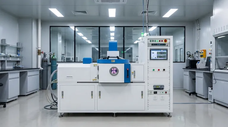
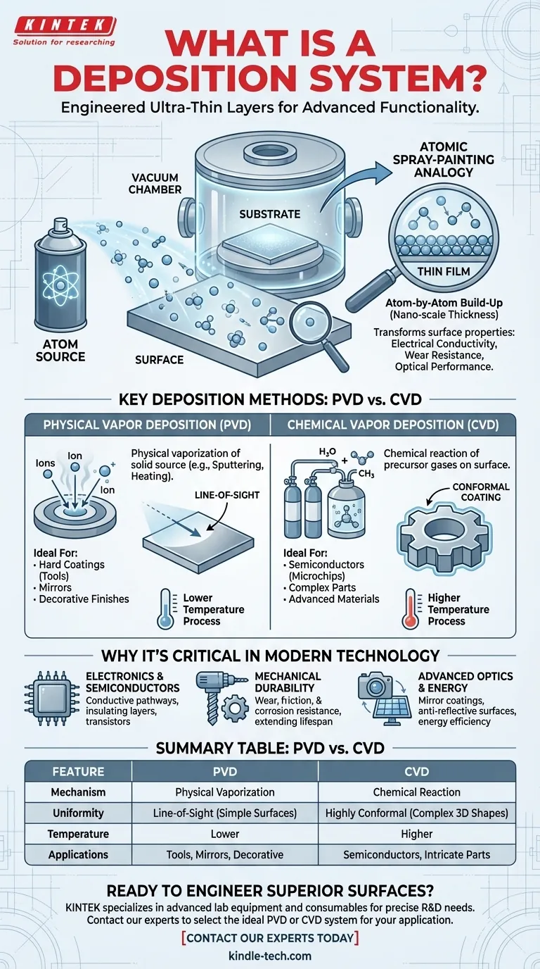
At their core, deposition systems are machines designed to apply an ultra-thin layer of material onto a surface, known as a substrate. This process, often occurring in a vacuum, builds a new functional layer atom-by-atom or molecule-by-molecule, creating a "thin film" that gives the underlying object entirely new properties.
The central purpose of a deposition system is not merely to coat an object, but to fundamentally change its surface characteristics. These systems are the invisible engines behind modern electronics, advanced optics, and high-performance materials, enabling properties like electrical conductivity, wear resistance, or specific light reflection where they did not exist before.
The Fundamental Principle: Building a New Surface
A deposition system works by transforming a solid or gas material into a vapor, which is then precisely directed onto a substrate where it condenses or reacts to form a solid film.
An Analogy: Atomic Spray-Painting
Think of it as a form of highly advanced spray-painting. Instead of paint droplets, the system uses a controlled stream of individual atoms or molecules. This allows for the creation of films that are exceptionally thin, pure, and uniform, often just a few nanometers thick.
The Goal: Enhanced Functionality
The resulting thin film is not just decorative. It is an engineered layer that imparts a specific function. A piece of plastic can be made electrically conductive, a steel tool can be made dramatically harder, and a piece of glass can be turned into a perfect mirror.
Key Deposition Methods
While there are many specific techniques, most commercial deposition systems fall into two primary categories: Physical Vapor Deposition (PVD) and Chemical Vapor Deposition (CVD).
Physical Vapor Deposition (PVD)
In PVD, a solid source material is vaporized through physical means, such as heating or bombarding it with ions (a process called sputtering). This vapor travels through a vacuum chamber and condenses onto the substrate, forming the film.
PVD is widely used for applying hard, wear-resistant coatings on cutting tools, creating reflective mirror coatings, and depositing conductive layers in electronics.
Chemical Vapor Deposition (CVD)
In CVD, the substrate is exposed to one or more volatile precursor gases. These gases react or decompose on the substrate's surface to produce the desired solid film.
CVD is essential in the semiconductor industry for creating the intricate, layered structures of microchips. It is also used to grow advanced materials like carbon nanotubes and to apply highly corrosion-resistant coatings.
Why Deposition is Critical in Modern Technology
Deposition systems are not niche laboratory tools; they are foundational to the production of countless high-tech products.
For Electronics and Semiconductors
Nearly every modern electronic device relies on thin films. Deposition systems are used to create the conductive metal pathways, the insulating dielectric layers, and the active semiconducting films that form transistors and integrated circuits.
For Mechanical Durability and Protection
Deposition creates surfaces that can withstand extreme conditions. Protective films deposited on automotive parts, industrial tools, and medical implants provide exceptional resistance to wear, friction, and corrosion, dramatically extending their lifespan and performance.
For Advanced Optics and Energy
These systems are used to manufacture a vast range of optical components. This includes mirror coatings, anti-reflective coatings on lenses and solar cells (to maximize light absorption), and complex interference coatings that reflect or transmit specific wavelengths of light.
Understanding the Trade-offs: PVD vs. CVD
Choosing between PVD and CVD depends entirely on the material, the substrate, and the desired outcome. There is no single "best" method.
PVD: A Line-of-Sight Process
PVD is typically a "line-of-sight" process, meaning it coats surfaces directly exposed to the vapor source. This makes it excellent for coating flat or gently curved surfaces but less effective for complex, three-dimensional shapes with hidden areas. It is generally a lower-temperature process, making it suitable for a wider range of substrate materials.
CVD: A Conformal Coating Process
Because CVD relies on gas that can flow around an object, it can produce a highly conformal coating that uniformly covers even very complex and intricate geometries. However, CVD often requires higher temperatures to drive the necessary chemical reactions, which can limit the types of substrates that can be used without being damaged.
Making the Right Choice for Your Goal
Your application's specific requirements will determine the ideal deposition technology.
- If your primary focus is surface hardness, decorative finishes, or mirror coatings on relatively simple shapes: PVD is often the most direct and cost-effective solution.
- If your primary focus is creating complex semiconductor devices or a perfectly uniform coating on an intricate 3D part: CVD is typically the required method due to its conformal nature.
- If your primary focus is research and development of new materials: Both PVD and CVD offer immense flexibility for creating films from metals, ceramics, and advanced compounds.
Ultimately, deposition systems are the unseen architects enabling the performance of the materials that define our modern technological world.
Summary Table:
| Feature | PVD (Physical Vapor Deposition) | CVD (Chemical Vapor Deposition) |
|---|---|---|
| Primary Mechanism | Vaporizes solid material physically (e.g., sputtering) | Uses chemical reactions from precursor gases |
| Coating Uniformity | Line-of-sight; best for simple, exposed surfaces | Highly conformal; excellent for complex 3D shapes |
| Typical Process Temp | Lower temperature | Higher temperature |
| Common Applications | Hard coatings for tools, mirror coatings, decorative finishes | Semiconductor devices, intricate part coatings, advanced materials |
Ready to Engineer Superior Surfaces?
Whether you are developing next-generation semiconductors, enhancing the durability of mechanical components, or creating advanced optical coatings, choosing the right deposition technology is critical to your success.
KINTEK specializes in advanced lab equipment and consumables, serving the precise needs of laboratories and R&D facilities. Our expertise can help you select the ideal PVD or CVD system to achieve the specific film properties—from conductivity and hardness to optical performance—that your project demands.
Contact our experts today to discuss your application requirements and discover how KINTEK's solutions can accelerate your innovation and ensure reliable, high-quality results.
Visual Guide
Related Products
- Chemical Vapor Deposition CVD Equipment System Chamber Slide PECVD Tube Furnace with Liquid Gasifier PECVD Machine
- RF PECVD System Radio Frequency Plasma-Enhanced Chemical Vapor Deposition RF PECVD
- Customer Made Versatile CVD Tube Furnace Chemical Vapor Deposition Chamber System Equipment
- Inclined Rotary Plasma Enhanced Chemical Vapor Deposition PECVD Equipment Tube Furnace Machine
- Inclined Rotary Plasma Enhanced Chemical Vapor Deposition PECVD Equipment Tube Furnace Machine
People Also Ask
- What is plasma enhanced chemical vapor deposition PECVD equipment? A Guide to Low-Temperature Thin Film Deposition
- What are the advantages of chemical vapor deposition? Achieve Superior Thin Films for Your Lab
- Why is Chemical Vapor Deposition (CVD) equipment uniquely suited for constructing hierarchical superhydrophobic structures?
- What are the core advantages of PE-CVD in OLED encapsulation? Protect Sensitive Layers with Low-Temp Film Deposition
- What types of substrates are used in CVD to facilitate graphene films? Optimize Graphene Growth with the Right Catalyst


