Dielectric Blocking Discharge Enhanced Chemical Vapour Deposition (DBD-PECVD), also widely recognized as dielectric barrier discharge or silent discharge, is a sophisticated method for creating thin films using non-equilibrium gas discharge.
Its defining characteristic is the insertion of an insulating medium directly into the discharge space. This modification allows the system to generate a stable, uniform plasma even at high pressures, making it a critical technology for the preparation of materials like silicon thin films.
Core Insight: DBD-PECVD effectively bridges the gap between different plasma technologies. It delivers the uniformity typically found in low-pressure glow discharges while maintaining the capability to operate at the high air pressures usually associated with corona discharges.
The Mechanics of the Discharge
The Role of the Insulating Medium
The fundamental innovation in this technique is the physical presence of a dielectric (insulating) barrier within the discharge gap.
This barrier limits the current in the discharge, preventing the formation of thermal sparks or arcs. By "blocking" the direct flow of current, the system forces the discharge to spread out, resulting in a non-equilibrium gas discharge.
Silent Discharge Characteristics
Because of the dielectric barrier, the discharge does not crackle or spark violently like an uninsulated high-voltage discharge.
This creates what is historically termed a silent discharge. It provides a controlled energetic environment necessary for chemical vapor deposition without the destructive thermal effects of an arc.
Bridging Discharge Technologies
Combining Uniformity and Pressure
Standard plasma technologies often force a choice between uniformity and operating pressure.
Glow discharges provide excellent uniformity but typically require low-pressure (vacuum) environments. Corona discharges operate at high pressures but are often non-uniform or localized.
The DBD Advantage
DBD-PECVD combines the best attributes of both predecessors.
It achieves the uniform discharge structure characteristic of a glow discharge. Simultaneously, it retains the ability to function effectively under high air pressure conditions, similar to a corona discharge.
Applications in Material Science
Silicon Thin Films
The primary application for DBD-PECVD cited in current research is the preparation of silicon thin films.
The ability to deposit these films at higher pressures can simplify manufacturing processes by reducing the need for complex high-vacuum equipment.
Understanding the Trade-offs
Process Complexity
While DBD-PECVD solves the pressure-uniformity conflict, introducing a dielectric barrier adds physical complexity to the reactor design.
The insulating medium must be robust enough to withstand the plasma environment without degrading and contaminating the thin film being deposited.
Energy Efficiency vs. Stability
Creating a non-equilibrium discharge at high pressure requires careful power management.
While the barrier prevents arcing, ensuring that the energy is efficiently coupled into the gas to drive the chemical deposition—rather than just generating heat in the dielectric—is a critical engineering balance.
Making the Right Choice for Your Goal
If you are evaluating DBD-PECVD for your thin-film deposition needs, consider the following operational priorities:
- If your primary focus is Film Uniformity: DBD offers a distinct advantage over standard high-pressure methods, providing a glow-like consistency across the substrate.
- If your primary focus is Operational Pressure: This technique allows you to bypass the strict low-vacuum requirements of traditional PECVD, enabling high-pressure processing.
DBD-PECVD stands out as a versatile solution for synthesizing silicon thin films when the constraints of traditional vacuum systems must be balanced against the need for high-quality, uniform coatings.
Summary Table:
| Feature | Low-Pressure Glow Discharge | Corona Discharge | DBD-PECVD |
|---|---|---|---|
| Operating Pressure | Low (Vacuum) | High | High (Atmospheric) |
| Uniformity | Excellent | Poor/Localized | Excellent (Glow-like) |
| Arc Prevention | Natural in vacuum | Low | Dielectric Barrier |
| Primary Application | Semiconductors | Surface Treatment | Silicon Thin Films |
Elevate Your Thin Film Deposition with KINTEK
Are you looking to bridge the gap between high-pressure efficiency and superior film uniformity? KINTEK specializes in advanced laboratory solutions, offering state-of-the-art CVD and PECVD systems tailored for cutting-edge material science. Whether you are researching silicon thin films or developing next-generation semiconductors, our expertise ensures you get the precise control your work demands.
Our comprehensive portfolio includes:
- Advanced Furnaces: Rotary, Vacuum, CVD, PECVD, and MPCVD systems.
- Precision Lab Equipment: High-temperature high-pressure reactors, autoclaves, and hydraulic presses.
- Research Consumables: PTFE products, high-purity ceramics, and specialized crucibles.
Ready to optimize your lab's performance? Contact KINTEK today to consult with our experts and find the perfect equipment for your research goals.
Related Products
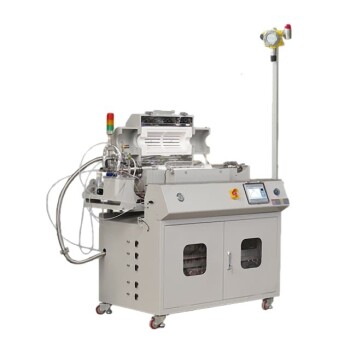
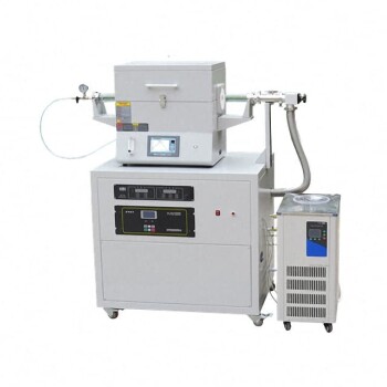
- Chemical Vapor Deposition CVD Equipment System Chamber Slide PECVD Tube Furnace with Liquid Gasifier PECVD Machine
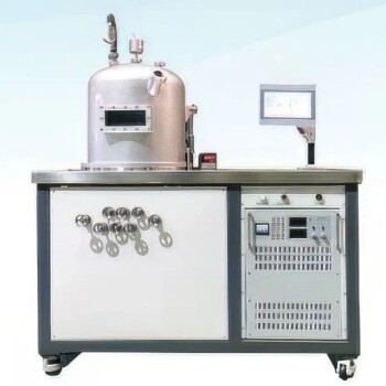
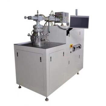
- RF PECVD System Radio Frequency Plasma-Enhanced Chemical Vapor Deposition RF PECVD
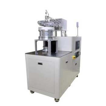
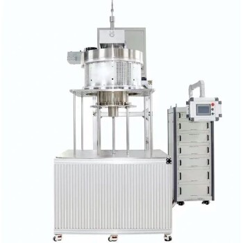
- Inclined Rotary Plasma Enhanced Chemical Vapor Deposition PECVD Equipment Tube Furnace Machine
- Inclined Rotary Plasma Enhanced Chemical Vapor Deposition PECVD Equipment Tube Furnace Machine
- CVD Diamond for Thermal Management Applications
People Also Ask
- Why is Chemical Vapor Deposition (CVD) equipment uniquely suited for constructing hierarchical superhydrophobic structures?
- What is plasma enhanced chemical vapor deposition PECVD equipment? A Guide to Low-Temperature Thin Film Deposition
- What are the advantages of chemical vapor deposition? Achieve Superior Thin Films for Your Lab
- What are the processes of vapor phase deposition? Understand CVD vs. PVD for Superior Thin Films
- What are the core advantages of PE-CVD in OLED encapsulation? Protect Sensitive Layers with Low-Temp Film Deposition
