In short, electron beam evaporation is a high-performance manufacturing process used to create extremely pure, high-quality thin film coatings. It is the go-to method for depositing materials with very high melting points or for applications in demanding industries like aerospace, optics, and semiconductors where coating performance is critical.
The core reason to use electron beam evaporation is its unique ability to vaporize virtually any material—especially those with high melting points—with extreme precision and minimal contamination, resulting in superior thin film quality that other methods cannot easily achieve.
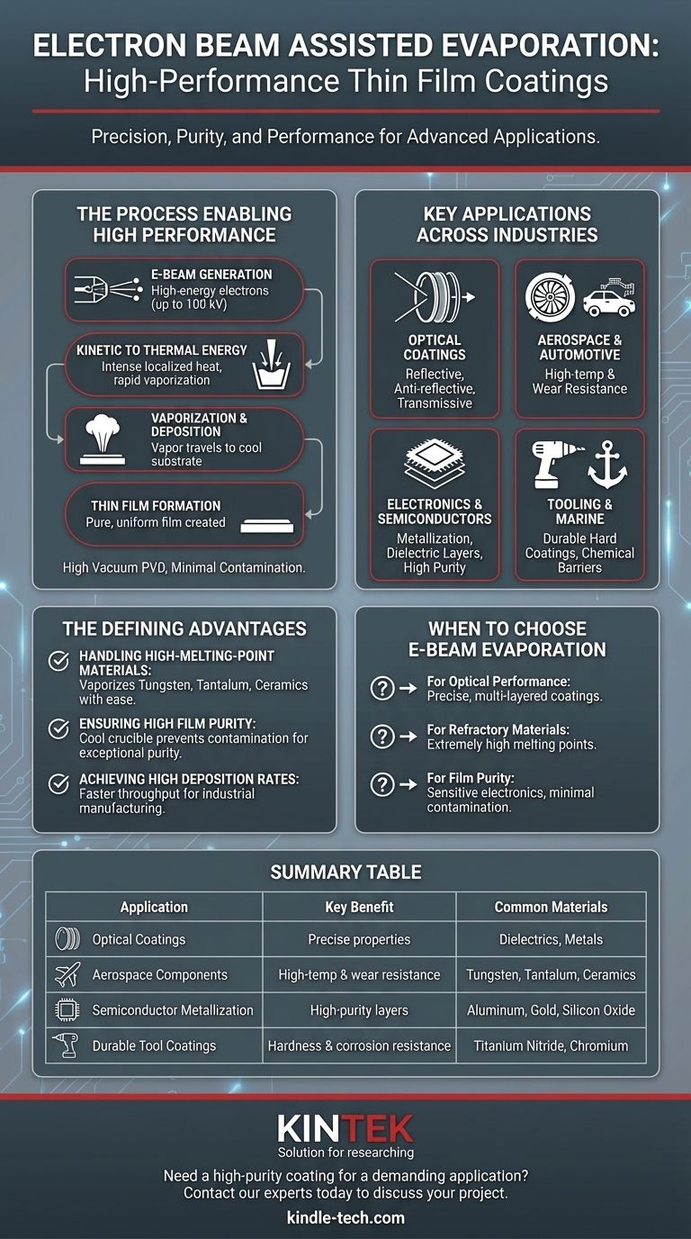
How the Process Enables High Performance
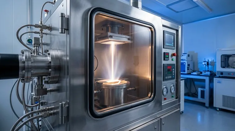
Electron beam evaporation is a type of physical vapor deposition (PVD) that operates under a high vacuum. Its distinct mechanism is what gives it a significant advantage for specialized applications.
The Core Mechanism
A powerful beam of high-energy electrons, often accelerated by voltages up to 100 kV, is generated and magnetically guided to strike a source material. This material, known as the evaporant, sits in a water-cooled crucible.
From Kinetic to Thermal Energy
The immense kinetic energy of the electrons is instantly converted into intense thermal energy upon impact with the source material. This creates a localized "hot spot" on the surface, causing it to rapidly heat up and vaporize.
Vaporization and Deposition
The resulting vapor travels in a straight line through the vacuum chamber and condenses onto a cooler substrate, forming a thin, uniform film. Because only the surface of the source material is heated, contamination from the crucible is virtually eliminated.
Key Applications Across Industries
The precision, purity, and versatility of e-beam evaporation make it essential for manufacturing advanced components that require specific material properties.
Optical Coatings
This is one of the most common uses. The process is ideal for creating multi-layer optical films for lenses, solar panels, eyeglasses, and architectural glass, providing precise reflective, anti-reflective, and transmissive qualities.
Aerospace and Automotive
In these industries, e-beam evaporation is used to apply high-temperature resistant and wear-resistant coatings to critical components like turbine blades and engine parts, significantly extending their operational lifespan and performance under extreme conditions.
Electronics and Semiconductors
The method is used for metallization and depositing dielectric layers in the fabrication of microelectronics. Its high purity is essential for creating reliable components like Josephson junctions and other advanced semiconductor devices.
Tooling and Marine Applications
For cutting tools, e-beam evaporation creates incredibly durable hard coatings that enhance sharpness and longevity. It also produces excellent chemical barriers to protect marine fittings and other parts from corrosion in harsh environments.
The Defining Advantages of E-Beam Evaporation
Engineers and scientists choose this method when the material or the application demands capabilities that other deposition techniques cannot offer.
Handling High-Melting-Point Materials
The intense, focused energy of the electron beam can vaporize materials that are impossible to melt with standard thermal evaporation, such as tungsten, tantalum, and various ceramics.
Ensuring High Film Purity
Because the electron beam heats the source material directly and the crucible remains cool, there is little to no risk of the crucible material leaching into the vapor. This results in an exceptionally pure final film.
Achieving High Deposition Rates
Compared to other PVD techniques like sputtering, e-beam evaporation can deposit material much more quickly. This high throughput is a significant advantage in many industrial manufacturing settings.
When to Choose E-Beam Evaporation
Selecting the right deposition method depends entirely on the material properties and performance requirements of your final product.
- If your primary focus is optical performance: E-beam is the superior choice for creating precise, multi-layered anti-reflective or reflective coatings with high purity.
- If your primary focus is depositing refractory metals or ceramics: The intense, localized heating of the electron beam makes it one of the few viable methods for materials with extremely high melting points.
- If your primary focus is film purity for sensitive electronics: Choose e-beam evaporation to minimize contamination and ensure the highest quality dielectric or conductive layers.
Ultimately, electron beam evaporation is the manufacturing process of choice when performance, purity, and the ability to work with difficult materials are non-negotiable.
Summary Table:
| Application | Key Benefit | Common Materials |
|---|---|---|
| Optical Coatings | Precise reflective/anti-reflective properties | Dielectrics, Metals |
| Aerospace Components | High-temperature & wear resistance | Tungsten, Tantalum, Ceramics |
| Semiconductor Metallization | High-purity conductive/dielectric layers | Aluminum, Gold, Silicon Oxide |
| Durable Tool Coatings | Enhanced hardness & corrosion resistance | Titanium Nitride, Chromium |
Need a high-purity coating for a demanding application?
KINTEK specializes in advanced lab equipment, including electron beam evaporation systems, to meet the stringent requirements of aerospace, semiconductor, and optical manufacturing. Our solutions are designed to help you achieve superior film quality, work with high-melting-point materials, and enhance your production efficiency.
Contact our experts today to discuss how our e-beam evaporation technology can benefit your specific project.
Visual Guide
Related Products
- Electron Beam Evaporation Coating Tungsten Crucible and Molybdenum Crucible for High Temperature Applications
- Electron Beam Evaporation Coating Gold Plating Tungsten Molybdenum Crucible for Evaporation
- Electron Beam Evaporation Coating Oxygen-Free Copper Crucible and Evaporation Boat
- Electron Beam Evaporation Coating Conductive Boron Nitride Crucible BN Crucible
- E Beam Crucibles Electron Gun Beam Crucible for Evaporation
People Also Ask
- What are the applications of e-beam evaporation? Achieve High-Purity Coatings for Optics & Electronics
- What is the deposition rate of e-beam evaporation? Control Thin Film Quality and Speed
- What materials are used in electron beam evaporation? Master High-Purity Thin Film Deposition
- What is e-beam evaporation used for? Precision Coating for Optics, Aerospace & Electronics
- What is the process of e-beam coating? Achieve High-Purity, Precise Thin Films for Your Lab


