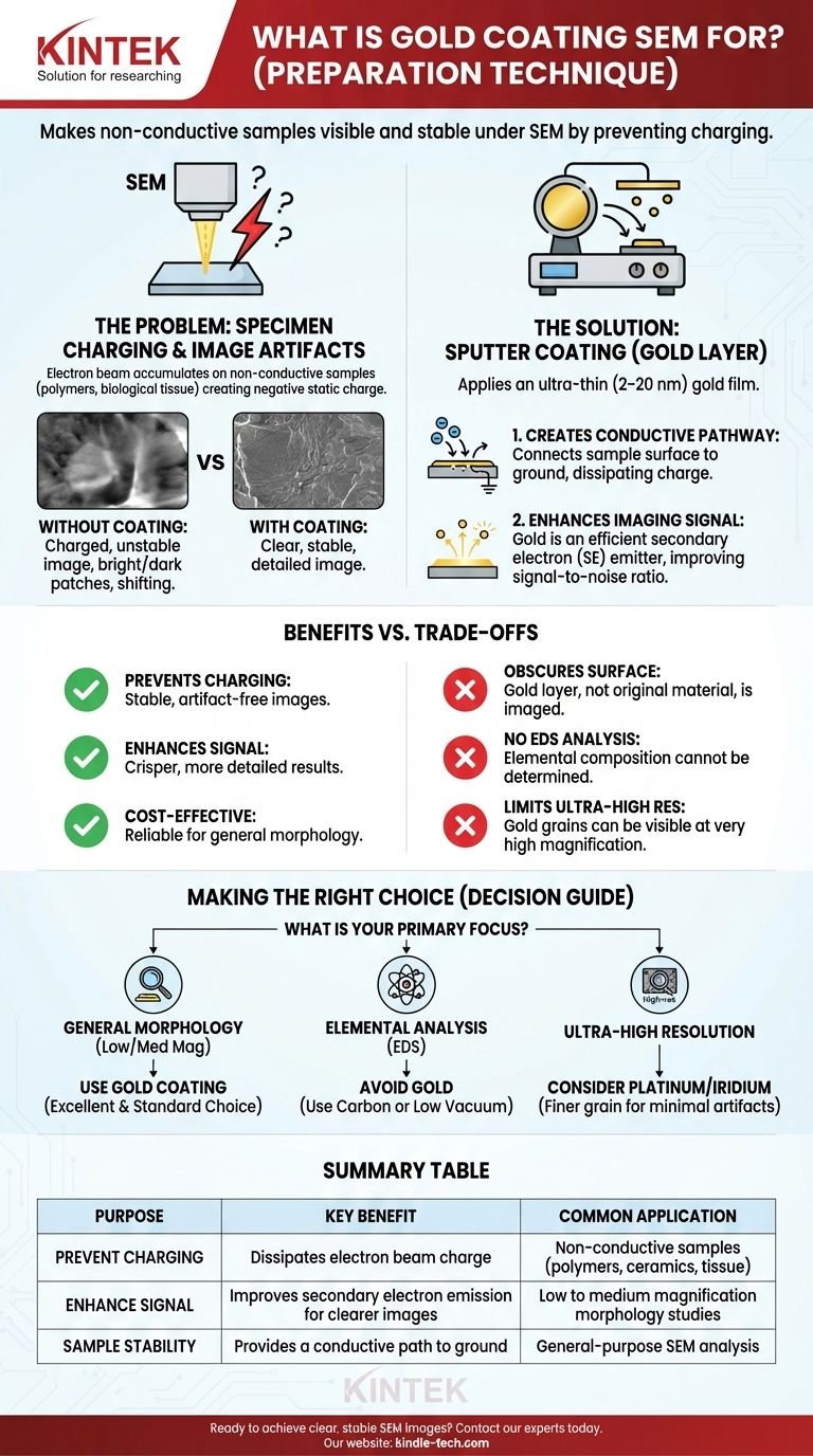
At its core, gold coating for SEM is a preparation technique that makes electrically non-conductive samples visible and stable under a scanning electron microscope (SEM). This process, known as sputter coating, applies an ultra-thin layer of gold to the specimen, preventing image-distorting electrical charges from building up and enhancing the signal used to create the final image.
The fundamental challenge of SEM is that the electron beam used for imaging will accumulate on non-conductive materials, creating a static charge that ruins the image. A micro-thin gold coating provides a conductive path for this charge to dissipate, effectively grounding the sample and enabling clear, stable analysis.
The Problem: Electron Beams and Non-Conductive Samples
To understand the need for gold coating, you must first understand the core interaction between an SEM and a non-conductive specimen.
What is "Specimen Charging"?
An SEM works by scanning a focused beam of high-energy electrons across a sample's surface.
When these electrons strike the material, they must have a path to ground. On a conductive material like metal, this happens automatically.
On a non-conductive or poorly-conductive sample (like polymers, ceramics, or biological tissue), the electrons accumulate on the surface, creating a negative static charge. This phenomenon is called specimen charging.
The Consequences of Charging
Specimen charging is disastrous for imaging. It creates severe visual artifacts that make the sample impossible to analyze accurately.
These artifacts include extremely bright or dark patches, image shifting and drifting, and a complete loss of surface detail.
How Gold Sputter Coating Solves the Problem
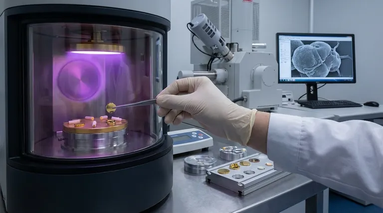
Sputter coating is the standard solution to specimen charging. It involves applying a metallic film, typically 2–20 nanometers thick, onto the sample.
Creating a Conductive Pathway
The primary function of the gold layer is to make the sample's surface electrically conductive.
This thin, continuous film connects the entire surface of the specimen to the aluminum stub it's mounted on, which is grounded to the SEM stage. This provides a path for incoming electrons to travel away, preventing any charge from building up.
Enhancing the Imaging Signal
A secondary, but crucial, benefit is the enhancement of the imaging signal. SEM images are most often formed by detecting secondary electrons (SE) that are emitted from the sample's surface.
Gold is a very efficient emitter of secondary electrons. The coating dramatically increases the number of SEs produced, which improves the signal-to-noise ratio and results in a crisper, clearer, and more detailed image.
Why Gold is a Common Choice
While other metals like platinum or iridium can be used, gold is a popular default for several reasons.
It has high electrical conductivity and is relatively easy and efficient to apply in a sputter coater. Its grain size is small enough to be unobtrusive for most low- and medium-magnification applications, making it a reliable and cost-effective choice.
Understanding the Trade-offs and Limitations
While essential, gold coating is not a perfect solution and comes with critical trade-offs that every analyst must consider.
The Original Surface is Obscured
The most significant disadvantage is that you are no longer imaging or analyzing the specimen's true surface. You are imaging the gold layer that conforms to it.
This makes techniques like Energy-Dispersive X-ray Spectroscopy (EDS), which determines elemental composition, impossible on the original material. The analysis will simply detect gold.
It Can Limit Ultra-High Resolution
For most tabletop or general-purpose SEMs, the resolution is not high enough to "see" the grain structure of the gold coating.
However, in high-performance SEMs working at very high magnifications, the gold grains themselves can become visible, obscuring the finest nanoscale features of the underlying sample.
Making the Right Choice for Your Analysis
Choosing the right surface preparation is critical for obtaining meaningful data. Your analytical goal should dictate your approach.
- If your primary focus is general morphology at low to medium magnification: Gold is an excellent, cost-effective, and standard choice for preventing charging and getting a clear image.
- If your primary focus is elemental surface analysis (EDS): You must avoid a metallic coating. Using a conductive carbon coating or analyzing the sample uncoated at low vacuum is necessary.
- If your primary focus is ultra-high-resolution imaging: You should consider a finer-grained (and more expensive) metal like platinum or iridium to minimize coating artifacts.
Ultimately, proper sample preparation is the foundation of high-quality electron microscopy.
Summary Table:
| Purpose | Key Benefit | Common Application |
|---|---|---|
| Prevent Charging | Dissipates electron beam charge | Non-conductive samples (polymers, ceramics, biological tissue) |
| Enhance Signal | Improves secondary electron emission for clearer images | Low to medium magnification morphology studies |
| Sample Stability | Provides a conductive path to ground | General-purpose SEM analysis |
Ready to achieve clear, stable SEM images?
Proper sample preparation is the foundation of high-quality electron microscopy. If you're working with non-conductive materials and need reliable results, KINTEK is here to help.
As your specialized partner in lab equipment and consumables, we provide the precise sputter coaters and expertise your laboratory needs to prevent charging and enhance your SEM analysis.
Contact our experts today to discuss your specific application and find the ideal solution for your lab!
Visual Guide
Related Products
People Also Ask
- What is e-beam evaporation? Achieve High-Purity Thin Film Deposition for Your Lab
- What materials are used in electron beam evaporation? Master High-Purity Thin Film Deposition
- What is the process of e-beam coating? Achieve High-Purity, Precise Thin Films for Your Lab
- What is the current of e-beam evaporation? A Guide to High-Purity Thin Film Deposition
- What is the temperature of e-beam evaporation? Mastering the Two-Zone Thermal Process for Precision Films
