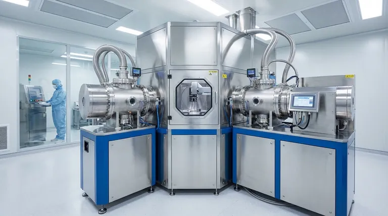
At its core, a Plasma-Enhanced Chemical Vapor Deposition (PECVD) cluster tool is an industrial workhorse used to deposit multiple, high-purity thin films onto a substrate in a single, continuous process. It is mission-critical for manufacturing complex devices like integrated circuits, solar cells, and advanced optical components where the integrity of interfaces between different material layers is paramount.
The central challenge in modern device fabrication is building complex, multi-layer structures without introducing performance-killing contaminants between each layer. A PECVD cluster tool solves this by integrating multiple deposition chambers into a single, high-vacuum environment, enabling the efficient and pristine creation of the advanced materials that power our technology.
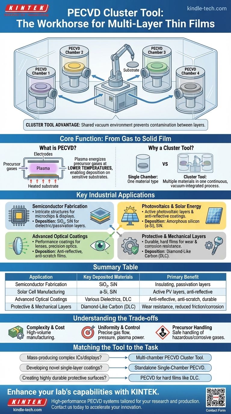
The Core Function: From Gas to Solid Film
To understand the applications, you must first understand the process and the specific advantage of the "cluster tool" configuration.
What is PECVD?
PECVD is a process used to deposit a thin, solid film from a gas state onto a substrate. Unlike traditional Chemical Vapor Deposition (CVD), which requires very high temperatures, PECVD uses a plasma to energize the precursor gases.
This plasma allows the chemical reactions to occur at much lower temperatures. This is critical when depositing films onto substrates that already contain sensitive, pre-existing electronic components that would be damaged by excessive heat.
Why a "Cluster Tool"?
A single PECVD chamber can deposit one type of material. A cluster tool, however, connects multiple process chambers (including several PECVD chambers) to a central robotic transfer module, all kept under a shared vacuum.
This design allows a substrate (like a silicon wafer) to be moved from one deposition chamber to the next without ever being exposed to the open air. This prevents oxygen, water vapor, and particulate contamination at the critical interfaces between different film layers, ensuring high device performance and yield.
Key Industrial Applications
The combination of low-temperature deposition and multi-layer capability makes PECVD cluster tools indispensable across several high-tech industries.
Semiconductor and Microelectronics Fabrication
This is the primary application. Cluster tools are used to build the intricate layered structures of integrated circuits (microchips) and flat-panel displays.
Common depositions include silicon dioxide (SiO₂) and silicon nitride (SiN), which serve as essential insulating (dielectric) layers, passivation layers to protect the device, and components of capacitors.
Photovoltaics and Solar Energy
In solar cell manufacturing, PECVD is used to deposit amorphous silicon (a-Si) films, which are the active photovoltaic material in many thin-film solar panels.
It is also used to create anti-reflective coatings (like silicon nitride) on the surface of crystalline silicon solar cells, maximizing the amount of light they absorb and increasing their overall efficiency.
Advanced Optical Coatings
PECVD is ideal for applying performance coatings to optical components like lenses, sunglasses, and precision instruments.
These films can serve as anti-scratch layers for durability or as precisely tuned anti-reflective coatings to improve light transmission.
Protective and Mechanical Layers
The process can create exceptionally hard and durable films. Diamond-Like Carbon (DLC) coatings are a prime example, deposited on mechanical parts to reduce wear, friction, and corrosion.
Similar protective coatings are used in demanding environments, from biomedical implants that require biocompatibility to industrial pipelines needing corrosion resistance.
Understanding the Trade-offs
While powerful, the PECVD cluster tool approach involves important considerations.
Complexity and Cost
Cluster tools are highly sophisticated and expensive pieces of capital equipment. Their operation and maintenance require significant expertise and investment, making them suitable primarily for high-volume manufacturing environments.
Uniformity and Control
Achieving a perfectly uniform film thickness and composition across a large substrate (e.g., a 300mm silicon wafer) is a constant challenge. It requires precise control over gas flow, pressure, plasma power, and temperature within the chamber.
Precursor Handling
The precursor gases used in PECVD can be hazardous, flammable, or corrosive. Safe and reliable handling, delivery, and exhaust management are critical operational and safety concerns.
Matching the Tool to the Task
Your choice of deposition technology depends entirely on the complexity and scale of your objective.
- If your primary focus is mass-producing complex integrated circuits or flat-panel displays: A multi-chamber PECVD cluster tool is the non-negotiable industry standard for achieving the required purity, throughput, and multi-layer capability.
- If your primary focus is developing novel single-layer coatings for R&D: A simpler, standalone single-chamber PECVD system is a far more practical and cost-effective choice.
- If your primary focus is creating highly durable protective surfaces: PECVD's ability to deposit hard films like DLC at low temperatures makes it superior for coating finished mechanical parts or heat-sensitive materials.
Ultimately, the PECVD cluster tool is a foundational technology that makes the high-volume manufacturing of modern electronic and optical devices possible.
Summary Table:
| Application | Key Deposited Materials | Primary Benefit |
|---|---|---|
| Semiconductor Fabrication | Silicon Dioxide (SiO₂), Silicon Nitride (SiN) | Creates insulating and passivation layers for microchips |
| Solar Cell Manufacturing | Amorphous Silicon (a-Si), Silicon Nitride (SiN) | Forms active photovoltaic layers and anti-reflective coatings |
| Advanced Optical Coatings | Various Dielectrics, Diamond-Like Carbon (DLC) | Provides anti-reflective, anti-scratch, and durable surfaces |
| Protective & Mechanical Layers | Diamond-Like Carbon (DLC) | Enhances wear resistance, reduces friction and corrosion |
Ready to enhance your lab's thin-film deposition capabilities?
KINTEK specializes in providing high-performance lab equipment and consumables, including PECVD systems tailored to your research and production needs. Whether you are developing next-generation semiconductors, efficient solar cells, or durable optical coatings, our expertise ensures you achieve superior film quality and process efficiency.
Contact us today via our contact form to discuss how our solutions can accelerate your innovation and deliver the precision your work demands.
Visual Guide
Related Products
- Inclined Rotary Plasma Enhanced Chemical Vapor Deposition PECVD Equipment Tube Furnace Machine
- Inclined Rotary Plasma Enhanced Chemical Vapor Deposition PECVD Equipment Tube Furnace Machine
- Chemical Vapor Deposition CVD Equipment System Chamber Slide PECVD Tube Furnace with Liquid Gasifier PECVD Machine
- RF PECVD System Radio Frequency Plasma-Enhanced Chemical Vapor Deposition RF PECVD
- CVD Diamond Dressing Tools for Precision Applications
People Also Ask
- What are the core advantages of PE-CVD in OLED encapsulation? Protect Sensitive Layers with Low-Temp Film Deposition
- What is the necessity of depositing a silicon nitride (SiNx) thin film using PECVD? Optimize QSSPC Lifetime Measurement
- What is plasma enhanced chemical vapour deposition PECVD used for? Enable Low-Temp Thin Films for Electronics & Solar
- What is Plasma Enhanced Chemical Vapor Deposition (PECVD)? High-Quality Film Deposition at Low Temperatures
- How does plasma enhance CVD? Unlock Low-Temperature, High-Quality Film Deposition


