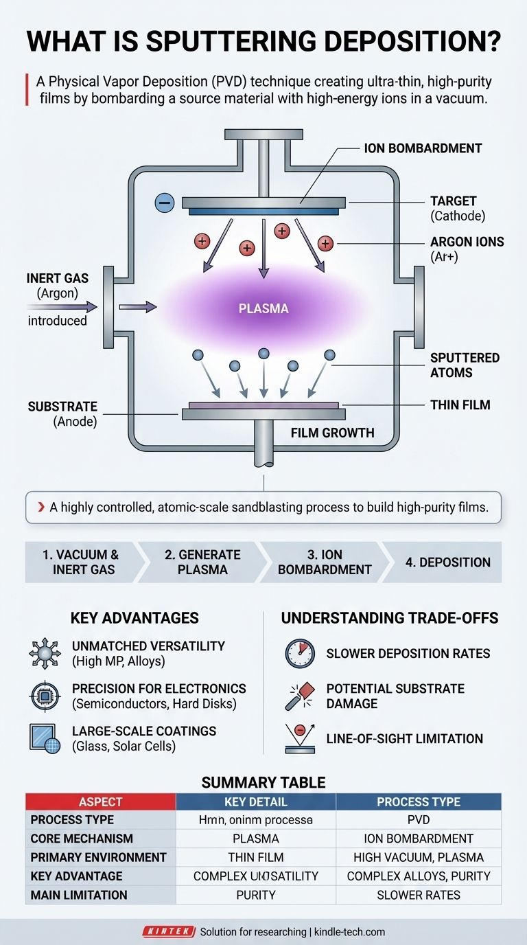
In essence, sputtering deposition is a physical vapor deposition (PVD) technique used to create ultra-thin films of material. The process works by bombarding a source material, known as the target, with high-energy ions inside a vacuum. This impact physically knocks atoms off the target, which then travel and deposit onto a nearby object, called the substrate, forming a uniform coating.
Sputtering is best understood as a highly controlled, atomic-scale sandblasting process. Instead of sand, it uses ions, and instead of eroding a surface, the ejected atoms are carefully collected to build a new, high-purity film on a different surface.
How Sputtering Works: A Step-by-Step Breakdown
To truly grasp the value of sputtering, we must look at its core mechanics. The entire process takes place within a sealed vacuum chamber, which is critical for ensuring the purity of the final film.
The Initial State: Vacuum and Inert Gas
First, the chamber is pumped down to a high vacuum to remove any contaminant particles like oxygen or water vapor. An inert gas, most commonly Argon, is then introduced at a very low pressure.
Generating the Plasma
A high voltage is applied between the target (acting as the cathode) and the chamber walls or a dedicated anode. This electrical field energizes the Argon gas, stripping electrons from the Argon atoms and creating a glowing, ionized gas known as a plasma. This plasma contains positively charged Argon ions (Ar+).
The Bombardment Phase
These positively charged Argon ions are accelerated by the electric field and smash into the negatively charged target material with immense energy.
This collision is purely physical, transferring momentum from the ion to the atoms on the target's surface. This energy transfer is powerful enough to knock out, or "sputter," individual atoms from the target.
Deposition: Building the Film
The sputtered atoms are ejected from the target and travel through the low-pressure vacuum chamber. They eventually strike the substrate—the object being coated, such as a silicon wafer or piece of glass—which is strategically placed nearby.
Upon arrival, these atoms condense on the substrate's surface, gradually building a thin film layer by layer. The thickness of this film can be controlled with extreme precision, from a few nanometers to several micrometers.
Key Applications and Advantages
Sputtering is not a niche laboratory method; it is a cornerstone of modern manufacturing due to its unique capabilities.
Unmatched Material Versatility
One of sputtering's greatest strengths is its ability to deposit materials that are otherwise very difficult to work with. This includes metals with extremely high melting points and complex alloys. Because the process is physical, not thermal, it can deposit these materials without altering their composition.
Precision for Advanced Electronics
The semiconductor and data storage industries rely heavily on sputtering. It is used to deposit the thin layers of conductive and magnetic materials required to produce integrated circuits and computer hard disks. The process's control and purity are essential for creating these microscopic, high-performance structures.
Large-Scale Industrial Coatings
Beyond electronics, sputtering is used to coat vast surfaces like architectural glass. These coatings can provide anti-reflective properties, thermal insulation, or specific colors. It is also fundamental to producing solar cells, optical media like CDs and DVDs, and durable decorative coatings on automotive parts.
Understanding the Trade-offs
No process is perfect. While powerful, sputtering has inherent limitations that make it unsuitable for certain applications.
Slower Deposition Rates
Compared to other methods like thermal evaporation, sputtering can be a slower process. The rate of material transfer is limited by the efficiency of the ion bombardment, which can increase production time and cost for very thick coatings.
Potential for Substrate Damage
The high-energy ions and sputtered atoms bombarding the substrate can sometimes cause damage, especially to sensitive organic or polymer-based materials. While this energy can improve film adhesion, it must be carefully managed.
Line-of-Sight Limitation
Sputtering is a line-of-sight process, meaning atoms generally travel in a straight line from the target to the substrate. This can make it challenging to achieve a uniform coating on objects with complex, three-dimensional shapes without sophisticated rotating fixtures.
Making the Right Choice for Your Goal
Selecting a deposition method depends entirely on the material properties and performance you need to achieve.
- If your primary focus is depositing a complex alloy or a high-purity film: Sputtering is an exceptional choice because it accurately preserves the target's stoichiometry.
- If your primary focus is coating a material with a very high melting point: Sputtering provides a reliable pathway where thermal evaporation would fail.
- If your primary focus is speed and cost for a simple, low-melting-point metal: You may find that a simpler process like thermal evaporation offers a more efficient solution.
Ultimately, sputtering deposition provides an unparalleled level of control for engineering surfaces at the atomic level.
Summary Table:
| Aspect | Key Detail |
|---|---|
| Process Type | Physical Vapor Deposition (PVD) |
| Core Mechanism | Ion bombardment (e.g., Ar+) knocks atoms from a target onto a substrate |
| Primary Environment | High vacuum chamber with inert gas plasma |
| Key Advantage | Deposits complex alloys & high-melting-point materials with high purity |
| Common Applications | Semiconductor circuits, hard disks, architectural glass, solar cells |
| Main Limitation | Slower deposition rates compared to some other PVD methods |
Need a reliable partner for your thin film deposition projects?
KINTEK specializes in high-performance lab equipment and consumables for precise coating applications. Whether you are developing next-generation semiconductors, optical coatings, or durable industrial finishes, our expertise in sputtering targets and deposition systems can help you achieve superior film quality, consistency, and material purity.
Contact our experts today to discuss how we can support your laboratory's specific needs and drive your R&D or production forward.
Visual Guide