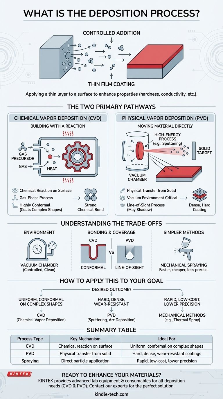
In the simplest terms, deposition is the process of applying a thin layer of material onto a surface. This process spans from natural geological phenomena, like sediment settling in a riverbed, to highly controlled industrial techniques used to create advanced coatings on materials. These techniques fundamentally involve moving atoms or molecules from a source and having them settle and bond to a target surface, known as a substrate.
The core concept of deposition is controlled addition. Whether through a chemical reaction, physical transfer, or mechanical application, the goal is always to build up a new layer of material on a base object to enhance its properties, such as hardness, conductivity, or corrosion resistance.
The Two Primary Deposition Pathways
At a high level, technical deposition processes are separated by how they move material onto the substrate. The distinction lies in whether the new layer is formed via a chemical reaction on the surface or by the physical transfer of the coating material itself.
Chemical Vapor Deposition (CVD): Building with a Reaction
In Chemical Vapor Deposition (CVD), the coating isn't transferred directly. Instead, the raw ingredients are introduced as a gas.
The part to be coated is placed inside a reaction chamber, often under vacuum. A volatile precursor gas containing the desired coating elements is then injected. When heated, this gas undergoes a chemical reaction or decomposition directly on the hot substrate's surface, forming a solid, thin film.
The key steps in CVD include the transport of gases to the surface, their adsorption, the surface reaction that forms the film, and the removal of gaseous by-products. This method creates a strong, chemically-bonded layer that can uniformly cover even complex shapes.
Physical Vapor Deposition (PVD): Moving Material Directly
In Physical Vapor Deposition (PVD), the coating material starts as a solid source (called a target). High-energy processes are used to transform this solid into a vapor, which then travels and condenses onto the substrate.
Two common PVD techniques illustrate this principle:
- Sputtering: A solid target is bombarded with high-energy ions in a vacuum. This impact acts like a microscopic sandblaster, knocking atoms off the target. These ejected atoms then travel and deposit onto the substrate, building the film atom by atom.
- Cathodic Arc Deposition: This technique uses a powerful electric arc to vaporize and ionize material from a solid cathode source. An electric field then accelerates these ions toward the substrate, where they condense to form an extremely dense and well-adhered coating.
Understanding the Trade-offs
Choosing a deposition method requires understanding the inherent differences in their approach, complexity, and the results they produce.
The Role of the Environment
Most advanced deposition techniques, like CVD and PVD, take place in a vacuum chamber. This controlled environment is critical for preventing contamination from air and for enabling the high-energy processes required to vaporize materials or facilitate specific chemical reactions.
Chemical vs. Physical Bonding
CVD forms the coating through a chemical reaction on the substrate, leading to a very strong chemical bond. Because the coating is formed from a gas that fills the chamber, it tends to be highly conformal, meaning it can evenly coat intricate and complex surfaces.
PVD, in contrast, is often a "line-of-sight" process. Atoms travel in a straight line from the source to the substrate, which can make it challenging to coat undercuts or the interior of complex geometries without sophisticated part manipulation.
Simpler Mechanical Methods
Not all deposition requires a vacuum or high-energy physics. Processes like spraying involve directing particles or droplets of the coating material onto the substrate. While simpler and less expensive, these methods typically offer less control over the coating's thickness, density, and adhesion compared to CVD or PVD.
How to Apply This to Your Goal
The best deposition process is entirely dependent on the desired outcome for the final product.
- If your primary focus is a highly uniform, pure, and chemically-bonded coating that covers complex shapes: CVD is often the superior choice due to its gas-phase, reaction-based nature.
- If your primary focus is depositing a very hard, dense, and wear-resistant coating from a solid metal or ceramic source: PVD techniques like sputtering or cathodic arc deposition are powerful industry standards.
- If your primary focus is a rapid, low-cost application where ultimate precision is not the main concern: Simpler methods like thermal spraying can be the most effective solution.
Understanding the fundamental mechanism—whether it's a chemical reaction or a physical transfer of atoms—is the key to selecting the right deposition process for any application.
Summary Table:
| Process Type | Key Mechanism | Ideal For |
|---|---|---|
| Chemical Vapor Deposition (CVD) | Chemical reaction on the substrate surface | Uniform, conformal coatings on complex shapes |
| Physical Vapor Deposition (PVD) | Physical transfer of atoms from a solid target | Hard, dense, wear-resistant coatings |
| Mechanical Methods (e.g., Spraying) | Direct application of particles/droplets | Rapid, low-cost applications where precision is less critical |
Ready to enhance your materials with the right deposition process?
KINTEK specializes in providing advanced lab equipment and consumables for all your deposition needs. Whether you require the uniform coverage of CVD or the durable coatings of PVD, our experts can help you select the perfect solution for your laboratory's specific challenges.
Contact us today to discuss how our deposition technologies can improve your material properties and drive your research forward!
Visual Guide
Related Products
- Aluminized Ceramic Evaporation Boat for Thin Film Deposition
- Tungsten Evaporation Boat for Thin Film Deposition
- Electron Beam Evaporation Coating Oxygen-Free Copper Crucible and Evaporation Boat
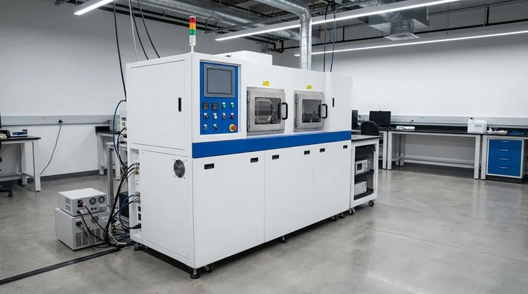
- HFCVD Machine System Equipment for Drawing Die Nano-Diamond Coating
- Molybdenum Tungsten Tantalum Evaporation Boat for High Temperature Applications
People Also Ask
- Why is an alumina boat and Ti3AlC2 powder bed necessary for Ti2AlC sintering? Protect MAX Phase Purity
- What is the source of evaporation for thin film? Choosing Between Thermal and E-Beam Methods
- Why are high-purity ceramic boats used for lignin activation? Ensure Purity & Thermal Stability
- What are thin films deposited by evaporation? A Guide to High-Purity Coating
- What is the chemical method for thin film deposition? Build Films from the Molecular Level Up


