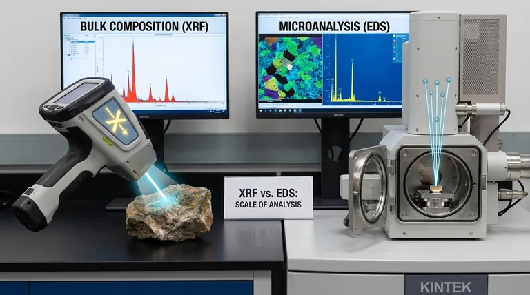
The fundamental difference between XRF and EDS lies in how the sample is energized and the scale of the analysis. Both techniques identify elements by reading characteristic X-rays emitted from a sample, but XRF uses an X-ray beam to analyze the bulk composition of a large area, while EDS uses an electron beam to analyze the microscopic composition of a tiny, specific point.
The choice between XRF and EDS is a choice of scale. XRF provides a fast, averaged chemical snapshot of a large sample area (the "forest"), while EDS provides a highly detailed chemical map of microscopic features within that sample (the "trees").
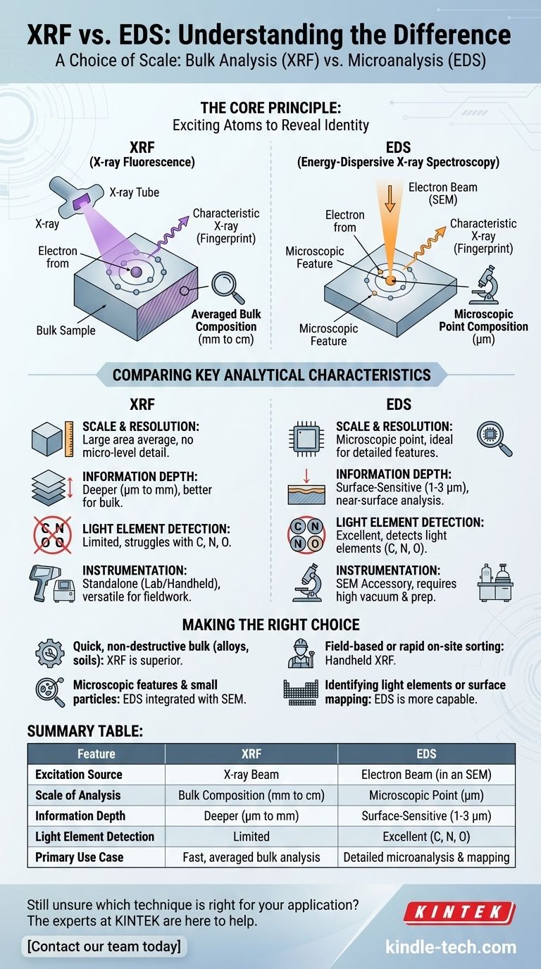
The Core Principle: Exciting Atoms to Reveal Identity
How Both Techniques Work
At the atomic level, both XRF and EDS operate on the same principle of atomic fluorescence.
A high-energy particle (either a photon from an X-ray tube or an electron from an electron beam) strikes an atom in your sample. This impact can knock an electron out of one of the atom's inner shells (e.g., the K or L shell).
This creates an unstable vacancy. To return to a stable state, an electron from a higher-energy outer shell drops down to fill the hole. The excess energy from this drop is released as an X-ray, whose energy is the precise difference between the two shells.
Because the energy levels of electron shells are unique to each element, the energy of this emitted X-ray acts as a distinct fingerprint, allowing us to identify the element it came from.
The Critical Difference: The Excitation Source
The practical distinction between the two methods comes entirely from the source used to create that initial electron vacancy.
X-ray Fluorescence (XRF) uses a primary beam of high-energy X-rays generated by an X-ray tube. These X-rays are photons, which penetrate the sample and excite a relatively large volume of atoms.
Energy-Dispersive X-ray Spectroscopy (EDS) uses a highly focused electron beam, typically generated inside a Scanning Electron Microscope (SEM). These electrons strike a very small, targeted spot on the sample's surface to generate the X-rays.
Comparing Key Analytical Characteristics
This single difference in the excitation source leads to profound differences in what each technique can tell you.
Scale of Analysis: Spatial Resolution
XRF analyzes a large area, with a spot size typically ranging from a few millimeters to several centimeters. It provides an average, bulk composition of the entire area being irradiated. You cannot use it to analyze a single, tiny crystal within a larger rock.
EDS analyzes a microscopic point, with a spot size that can be smaller than one micrometer. It provides the elemental composition of a specific feature you target using the microscope's image, making it ideal for microanalysis.
Information Depth
XRF is generally more penetrating. The incoming X-rays can travel deeper into the material, providing information from a depth of several micrometers to even millimeters, depending on the material's density. This reinforces its strength in bulk analysis.
EDS is inherently surface-sensitive. The electron beam interacts with a much smaller volume near the sample surface, typically analyzing a depth of only 1-3 micrometers. The results may not represent the material's overall bulk composition if the surface is altered or coated.
Elemental Range and Sensitivity
Both techniques are excellent for detecting elements from sodium (Na) upwards in the periodic table.
EDS, especially with modern windowless detectors, has a distinct advantage in detecting light elements like carbon (C), nitrogen (N), and oxygen (O). Standard XRF cannot detect these very light elements because their low-energy X-rays are absorbed by the air and the detector window.
XRF often provides better sensitivity for bulk measurements, capable of detecting elements down to the parts-per-million (ppm) range. EDS sensitivity is typically in the range of 0.1 weight percent.
Instrumentation and Practical Considerations
The XRF Spectrometer: A Standalone Instrument
XRF systems are self-contained instruments, ranging from large, high-power laboratory units to convenient handheld "pXRF" analyzers. This portability makes XRF invaluable for fieldwork, scrap metal sorting, and consumer product screening.
The EDS System: An SEM Accessory
An EDS detector is not a standalone device. It is almost always an accessory attached to a Scanning Electron Microscope (SEM) or Transmission Electron Microscope (TEM). The primary purpose of the SEM is high-magnification imaging; EDS adds the crucial capability of chemical analysis to those images.
Sample Requirements
XRF is extremely flexible and often non-destructive. It can analyze solids, liquids, powders, and films with minimal to no sample preparation.
EDS has stricter requirements. Samples must be solid, stable in a high vacuum, and small enough to fit in the SEM chamber. Non-conductive samples typically must be coated with a thin layer of carbon or gold to prevent charging, which can complicate the analysis of light elements.
Understanding the Trade-offs
XRF: Averaging and Matrix Effects
The primary limitation of XRF is its lack of spatial resolution. It gives you one averaged result for a large area, meaning you could miss critical variations in composition at the micro-level. Results can also be influenced by "matrix effects," where the signal from one element is absorbed or enhanced by other elements in the sample.
EDS: Surface Focus and Vacuum Constraints
The main drawback of EDS is that it only analyzes the near-surface of a sample, which may not be representative of the bulk material. Furthermore, the requirement for samples to be vacuum-compatible and often conductively coated excludes many sample types and can interfere with results.
Making the Right Choice for Your Goal
Your analytical question dictates the correct tool.
- If your primary focus is quick, non-destructive bulk composition of large samples (like alloys, soils, or polymers): XRF is the superior choice for its speed and simplicity.
- If your primary focus is analyzing the chemical composition of microscopic features, small particles, or different phases in a material: EDS integrated with an SEM is the only viable option.
- If your primary focus is field-based analysis or rapid material sorting on-site: Handheld XRF provides unmatched portability and immediate results.
- If your primary focus is identifying light elements (like C, N, O) or creating elemental maps of a surface: EDS is significantly more capable than standard XRF.
Ultimately, your choice is determined by whether you need to understand the average composition of the whole or the specific makeup of its individual parts.
Summary Table:
| Feature | XRF (X-ray Fluorescence) | EDS (Energy-Dispersive X-ray Spectroscopy) |
|---|---|---|
| Excitation Source | X-ray Beam | Electron Beam (in an SEM) |
| Scale of Analysis | Bulk Composition (mm to cm) | Microscopic Point (µm) |
| Information Depth | Deeper (µm to mm) | Surface-Sensitive (1-3 µm) |
| Light Element Detection | Limited | Excellent (C, N, O) |
| Primary Use Case | Fast, averaged bulk analysis | Detailed microanalysis & mapping |
Still unsure which technique is right for your application? The experts at KINTEK are here to help. We specialize in providing the right lab equipment and consumables to meet your specific analytical challenges. Whether you need robust XRF spectrometers for bulk material analysis or sophisticated SEM-EDS systems for microanalysis, we have the solution.
Contact our team today to discuss your requirements and discover how KINTEK can enhance your laboratory's capabilities and efficiency.
Visual Guide
Related Products
- Laboratory Test Sieves and Vibratory Sieve Shaker Machine
- RF PECVD System Radio Frequency Plasma-Enhanced Chemical Vapor Deposition RF PECVD
- Customizable PEM Electrolysis Cells for Diverse Research Applications
- Laboratory Disc Rotary Mixer for Efficient Sample Mixing and Homogenization
- Laboratory Multifunctional Small Speed-Adjustable Horizontal Mechanical Shaker for Lab
People Also Ask
- What can be separated by sieving? A Guide to Particle Size Separation for Various Materials
- What is the operating procedure of a sieve shaker? Master Accurate Particle Size Analysis
- What is the maximum sieving deviation permitted? A Guide to ASTM & ISO Precision Limits
- What is the principle of sieving machine? Achieve Accurate Particle Size Separation
- What size are test sieves? A Guide to Frame Diameters and Mesh Sizes