Knowledge What is the process used in semiconductor device fabrication? A Step-by-Step Guide to Microchip Manufacturing
Author avatar

Tech Team · Kintek Solution

Updated 23 hours ago

What is the process used in semiconductor device fabrication? A Step-by-Step Guide to Microchip Manufacturing


At its core, semiconductor device fabrication is a cyclical manufacturing process that uses light, chemicals, and specialized materials to build microscopic, three-dimensional electronic circuits layer by layer on a silicon wafer. A typical cycle involves depositing a material layer, applying a light-sensitive coating (photoresist), using a light pattern to harden specific areas, and then chemically etching away the unwanted material to create a feature. This entire sequence is repeated hundreds of times to construct complex devices like transistors and integrated circuits.

The central concept to grasp is that semiconductor fabrication is not a single assembly line, but rather a form of microscopic, additive and subtractive 3D printing. The process repeatedly adds new material layers and then precisely carves patterns into them, gradually building the intricate architecture of a modern microchip.

What is the process used in semiconductor device fabrication? A Step-by-Step Guide to Microchip Manufacturing

The Foundation: From Sand to Silicon Wafer

The Starting Material

Nearly all modern semiconductor devices, from transistors to complex processors, begin life as a thin, perfectly flat disc called a silicon wafer.

These wafers are produced by growing a massive, single crystal of ultra-pure silicon, which is then sliced into discs and polished to an atomic-level smoothness. This pristine surface is the canvas upon which all circuitry is built.

The Goal: Building Transistors

The ultimate goal of fabrication is to create billions of microscopic switches called transistors (like FETs or BJTs) and connect them with metal wiring. These transistors are the fundamental building blocks of all digital logic and memory.

The Core Fabrication Cycle: Sculpting with Light and Chemicals

The creation of a circuit is not a single process, but a loop that can be repeated hundreds of times. Each cycle adds a new layer of complexity to the device.

Step 1: Deposition (Adding a Layer)

First, a thin film of a specific material is uniformly deposited across the entire wafer surface. This material could be an insulator (like silicon dioxide), a conductor (like copper), or another semiconductor material.

For example, a layer of silicon nitride might be added using chemical vapor deposition (CVD), a process that can involve ammonia gas as a precursor. This creates a new, blank slate for the next pattern.

Step 2: Photolithography (Creating the Blueprint)

This is the most critical step, where the circuit design is transferred to the wafer. It involves coating the wafer with a light-resistant chemical called photoresist.

A mask, which acts like a stencil for the circuit pattern, is placed between a UV light source and the wafer. When the light shines, it selectively hardens (or softens, depending on the process) the photoresist, creating a precise pattern.

Step 3: Etching (Removing Material)

The wafer is then exposed to chemicals or plasma that etch away the material not protected by the hardened photoresist pattern.

This transfers the 2D pattern from the photoresist into the 3D material layer underneath. The photoresist acts as a temporary mask, ensuring only the desired parts of the underlying film are removed.

Step 4: Stripping (Cleaning the Slate)

Finally, the remaining photoresist is completely removed or "stripped" from the wafer using solvents or plasma.

This leaves behind a wafer with a newly patterned layer of material. The wafer is now clean and ready to begin the entire cycle again with a new deposition step.

Understanding the Trade-offs and Challenges

The elegance of this process hides immense engineering complexity. Success depends on navigating critical physical and chemical limitations.

The Precision Problem: Alignment and Resolution

Each new layer must be aligned to the one beneath it with nanometer-level accuracy. A slight misalignment over hundreds of layers can render the entire chip non-functional. Furthermore, the laws of physics limit how small a pattern can be projected with light.

The Gap-Filling Challenge

As components are built vertically, tiny, high-aspect-ratio gaps form between them. Filling these gaps with an insulating or conductive material without creating voids is a major challenge. Voids can trap charge or block electrical signals, causing device failure.

The Purity Imperative: Contamination Control

The entire fabrication process occurs in a "cleanroom," one of the most sterile environments on Earth. A single speck of dust is a boulder on the microscopic scale of a transistor and can easily destroy a chip, causing a defect that ruins the final product.

Key Principles for Your Understanding

To truly grasp the essence of semiconductor fabrication, focus on the underlying goals rather than memorizing a single sequence of steps.

  • If your primary focus is the overall process: Remember that it's a highly repetitive cycle of Deposition, Lithography, Etch, and Strip used to build a 3D structure from the ground up.
  • If your primary focus is on how circuits are designed: Understand that photolithography is the key step that transfers an engineer's digital design (encoded on a mask) into a physical pattern on the wafer.
  • If your primary focus is on the physical device: View the process as a sophisticated sculpting technique, where layers are repeatedly added and carved away to create the functional architecture of transistors and their interconnections.

Ultimately, semiconductor fabrication is the engine that transforms human design into the physical reality of the digital world.

Summary Table:

Step Process Key Action Purpose
1 Deposition Adding a material layer (e.g., via CVD) Creates a new, uniform surface for patterning
2 Photolithography Using UV light and a mask to pattern photoresist Transfers circuit design onto the wafer
3 Etching Removing unprotected material (e.g., with chemicals/plasma) Carves the pattern into the underlying layer
4 Stripping Removing leftover photoresist Cleans the wafer for the next cycle

Ready to Elevate Your Semiconductor Research or Production?

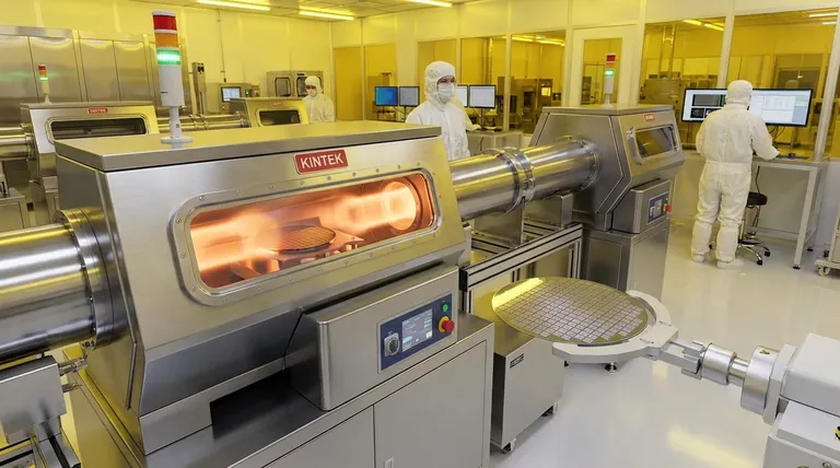
Building reliable microchips demands precision equipment and high-purity consumables. KINTEK specializes in providing the essential lab equipment and materials that semiconductor fabrication depends on—from deposition systems to etching tools and ultra-clean consumables.

Let us help you achieve nanometer-scale accuracy and contamination-free results. Contact our experts today to discuss how KINTEK’s solutions can support your laboratory’s semiconductor device fabrication needs.

Visual Guide

What is the process used in semiconductor device fabrication? A Step-by-Step Guide to Microchip Manufacturing Visual Guide

Related Products

People Also Ask

Related Products

Chemical Vapor Deposition CVD Equipment System Chamber Slide PECVD Tube Furnace with Liquid Gasifier PECVD Machine

Chemical Vapor Deposition CVD Equipment System Chamber Slide PECVD Tube Furnace with Liquid Gasifier PECVD Machine

KT-PE12 Slide PECVD System: Wide power range, programmable temp control, fast heating/cooling with sliding system, MFC mass flow control & vacuum pump.

Inclined Rotary Plasma Enhanced Chemical Vapor Deposition PECVD Equipment Tube Furnace Machine

Inclined Rotary Plasma Enhanced Chemical Vapor Deposition PECVD Equipment Tube Furnace Machine

Upgrade your coating process with PECVD coating equipment. Ideal for LED, power semiconductors, MEMS and more. Deposits high-quality solid films at low temps.

RF PECVD System Radio Frequency Plasma-Enhanced Chemical Vapor Deposition RF PECVD

RF PECVD System Radio Frequency Plasma-Enhanced Chemical Vapor Deposition RF PECVD

RF-PECVD is an acronym for "Radio Frequency Plasma-Enhanced Chemical Vapor Deposition." It deposits DLC (Diamond-like carbon film) on germanium and silicon substrates. It is utilized in the 3-12um infrared wavelength range.

Customer Made Versatile CVD Tube Furnace Chemical Vapor Deposition Chamber System Equipment

Customer Made Versatile CVD Tube Furnace Chemical Vapor Deposition Chamber System Equipment

Get your exclusive CVD furnace with KT-CTF16 Customer Made Versatile Furnace. Customizable sliding, rotating, and tilting functions for precise reactions. Order now!

Vacuum Hot Press Furnace Machine for Lamination and Heating

Vacuum Hot Press Furnace Machine for Lamination and Heating

Experience clean and precise lamination with Vacuum Lamination Press. Perfect for wafer bonding, thin-film transformations, and LCP lamination. Order now!

Electron Beam Evaporation Coating Oxygen-Free Copper Crucible and Evaporation Boat

Electron Beam Evaporation Coating Oxygen-Free Copper Crucible and Evaporation Boat

Electron Beam Evaporation Coating Oxygen-Free Copper Crucible enables precise co-deposition of various materials. Its controlled temperature and water-cooled design ensure pure and efficient thin film deposition.

1200℃ Split Tube Furnace with Quartz Tube Laboratory Tubular Furnace

1200℃ Split Tube Furnace with Quartz Tube Laboratory Tubular Furnace

KT-TF12 split tube furnace: high-purity insulation, embedded heating wire coils, and max. 1200C. Widely used for new materials and chemical vapour deposition.

CVD Diamond for Thermal Management Applications

CVD Diamond for Thermal Management Applications

CVD diamond for thermal management: High-quality diamond with thermal conductivity up to 2000 W/mK, ideal for heat spreaders, laser diodes, and GaN on Diamond (GOD) applications.

Laboratory Quartz Tube Furnace Tubular RTP Heating Furnace

Laboratory Quartz Tube Furnace Tubular RTP Heating Furnace

Get lightning-fast heating with our RTP Rapid Heating Tube Furnace. Designed for precise, high-speed heating and cooling with convenient sliding rail and TFT touch screen controller. Order now for ideal thermal processing!

1400℃ Laboratory Quartz Tube Furnace with Alumina Tube Tubular Furnace

1400℃ Laboratory Quartz Tube Furnace with Alumina Tube Tubular Furnace

Looking for a tube furnace for high-temperature applications? Our 1400℃ Tube Furnace with Alumina Tube is perfect for research and industrial use.

High Temperature Muffle Oven Furnace for Laboratory Debinding and Pre Sintering

High Temperature Muffle Oven Furnace for Laboratory Debinding and Pre Sintering

KT-MD High temperature debinding and pre-sintering furnace for ceramic materials with various molding processes. Ideal for electronic components such as MLCC and NFC.

1700℃ Laboratory Quartz Tube Furnace with Alumina Tube Tubular Furnace

1700℃ Laboratory Quartz Tube Furnace with Alumina Tube Tubular Furnace

Looking for a high-temperature tube furnace? Check out our 1700℃ Tube Furnace with Alumina Tube. Perfect for research and industrial applications up to 1700C.

Vacuum Sealed Continuous Working Rotary Tube Furnace Rotating Tube Furnace

Vacuum Sealed Continuous Working Rotary Tube Furnace Rotating Tube Furnace

Experience efficient material processing with our vacuum-sealed rotary tube furnace. Perfect for experiments or industrial production, equipped with optional features for controlled feeding and optimized results. Order now.

Rotary Tube Furnace Split Multi Heating Zone Rotating Tube Furnace

Rotary Tube Furnace Split Multi Heating Zone Rotating Tube Furnace

Multi zone rotary furnace for high-precision temperature control with 2-8 independent heating zones. Ideal for lithium ion battery electrode materials and high-temperature reactions. Can work under vacuum and controlled atmosphere.

VHP Sterilization Equipment Hydrogen Peroxide H2O2 Space Sterilizer

VHP Sterilization Equipment Hydrogen Peroxide H2O2 Space Sterilizer

A hydrogen peroxide space sterilizer is a device that uses vaporized hydrogen peroxide to decontaminate enclosed spaces. It kills microorganisms by damaging their cellular components and genetic material.

1800℃ Muffle Oven Furnace for Laboratory

1800℃ Muffle Oven Furnace for Laboratory

KT-18 muffle furnace with Japan Al2O3 polycrystalline fibe and Silicon Molybdenum heating element, up to 1900℃, PID temperature control and 7" smart touch screen. Compact design, low heat loss, and high energy efficiency. Safety interlock system and versatile functions.

Non Consumable Vacuum Arc Induction Melting Furnace

Non Consumable Vacuum Arc Induction Melting Furnace

Explore the benefits of Non-Consumable Vacuum Arc Furnace with high melting point electrodes. Small, easy to operate & eco-friendly. Ideal for laboratory research on refractory metals & carbides.

1700℃ Muffle Oven Furnace for Laboratory

1700℃ Muffle Oven Furnace for Laboratory

Get superior heat control with our 1700℃ Muffle Furnace. Equipped with intelligent temperature microprocessor, TFT touch screen controller & advanced insulation materials for precise heating up to 1700C. Order now!

1400℃ Muffle Oven Furnace for Laboratory

1400℃ Muffle Oven Furnace for Laboratory

Get precise high-temperature control up to 1500℃ with KT-14M Muffle furnace. Equipped with a smart touch screen controller and advanced insulation materials.

High Performance Laboratory Freeze Dryer for Research and Development

High Performance Laboratory Freeze Dryer for Research and Development

Advanced laboratory freeze dryer for lyophilization, preserving sensitive samples with precision. Ideal for biopharmaceuticals, research & food industries.


Leave Your Message