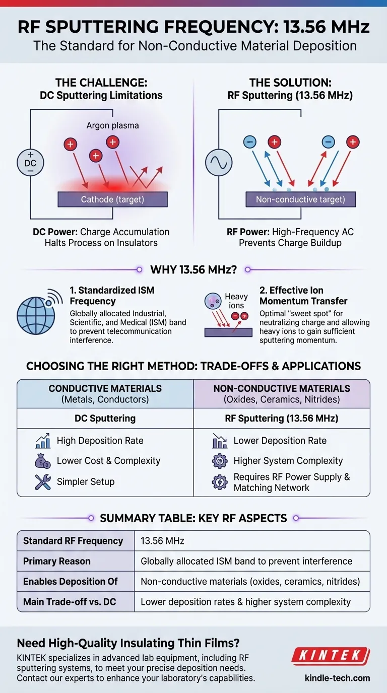
The standard radio frequency (RF) for sputtering is 13.56 MHz. This specific frequency is not chosen for performance reasons alone; it is a globally allocated Industrial, Scientific, and Medical (ISM) band. Using this standard prevents sputtering equipment from interfering with critical telecommunication services.
The core challenge in sputtering is that direct current (DC) methods only work on conductive materials. RF sputtering overcomes this by using an alternating current, which prevents electrical charge from building up on non-conductive targets and stopping the process.
Why RF is Necessary for Sputtering Certain Materials
To understand the role of RF, we must first look at the fundamental limitation of the simpler, more common DC sputtering method.
The Limitation of DC Sputtering
In any sputtering process, a target material is bombarded by positive ions (typically from an inert gas like argon) to dislodge atoms, which then deposit onto a substrate.
With a conductive target, a DC power supply works perfectly. The positive charge from the arriving ions is safely conducted away.
However, if the target is an electrical insulator (like a ceramic or oxide), this positive charge accumulates on the surface. This buildup quickly repels incoming positive ions, effectively halting the sputtering process entirely.
How RF Overcomes Charge Buildup
RF sputtering solves this problem by replacing the DC power supply with a high-frequency AC source.
The rapidly alternating voltage prevents a net positive charge from ever accumulating on the target's surface. During one half-cycle, the surface attracts positive ions for sputtering, and during the other, it attracts electrons which neutralize the built-up charge.
Frequencies of 1 MHz or higher are required for this effect to work. At these speeds, the current flows through the insulating target as if it were a capacitor, enabling the continuous deposition of non-conductive materials.
The Significance of the 13.56 MHz Frequency
While any frequency above 1 MHz can enable the sputtering of insulators, the choice of 13.56 MHz is deliberate and based on two key factors.
A Standardized ISM Frequency
The primary reason for using 13.56 MHz is regulatory. The International Telecommunication Union (ITU) designates specific frequencies for Industrial, Scientific, and Medical (ISM) purposes.
Using this approved frequency ensures that the high-power RF energy generated by the sputtering system does not interfere with radio, television, or other communication signals.
Effective for Ion Momentum Transfer
The 13.56 MHz frequency also sits in a practical "sweet spot." It is high enough to effectively neutralize charge on the insulating target.
Simultaneously, it is considered low enough to allow the relatively heavy argon ions in the plasma to respond to the electric field and gain sufficient momentum to strike the target, ensuring an efficient sputtering process.
Understanding the Trade-offs
While essential for depositing insulators, RF sputtering is not always the optimal choice. It comes with specific trade-offs compared to its DC counterpart.
Lower Deposition Rates
RF sputtering often has lower deposition rates than DC magnetron sputtering. This is partly because fewer secondary electrons are effectively trapped near the target to help ionize the sputtering gas, which can reduce the overall efficiency of the process.
Increased System Complexity
An RF sputtering system is inherently more complex than a DC system. It requires a sophisticated RF power supply and an impedance matching network to efficiently deliver power to the plasma chamber, which can increase the cost and maintenance requirements of the equipment.
Choosing the Right Sputtering Method
Your choice between RF and DC sputtering should be guided entirely by the electrical properties of your target material.
- If your primary focus is depositing conductive materials (metals, transparent conductors): DC sputtering is almost always the better choice due to its higher deposition rates, lower cost, and simpler setup.
- If your primary focus is depositing non-conductive materials (oxides, nitrides, ceramics): RF sputtering is the necessary and correct method, as it is designed specifically to overcome the issue of surface charging.
Ultimately, understanding the electrical nature of your target material dictates the correct sputtering technology to use.
Summary Table:
| Aspect | Key Information |
|---|---|
| Standard RF Frequency | 13.56 MHz |
| Primary Reason | Globally allocated ISM band to prevent interference |
| Enables Deposition Of | Non-conductive materials (oxides, ceramics, nitrides) |
| Main Trade-off vs. DC | Lower deposition rates and higher system complexity |
Need to deposit high-quality insulating thin films?
RF sputtering is essential for working with non-conductive targets. KINTEK specializes in advanced lab equipment, including RF sputtering systems, to meet your precise deposition needs for materials research and development.
Contact our experts today to discuss how our reliable sputtering solutions can enhance your laboratory's capabilities and accelerate your project success.
Visual Guide
Related Products
People Also Ask
- Why is a Matching Network Indispensable in RF-PECVD for Siloxane Films? Ensure Stable Plasma and Uniform Deposition
- What is plasma enhanced chemical vapour deposition PECVD used for? Enable Low-Temp Thin Films for Electronics & Solar
- What is plasma chemical vapor deposition? A Low-Temperature Thin Film Coating Solution
- What is an example of PECVD? RF-PECVD for High-Quality Thin Film Deposition
- How does Radio Frequency Enhanced Plasma Chemical Vapour Deposition (RF-PECVD) work? Learn the Core Principles
