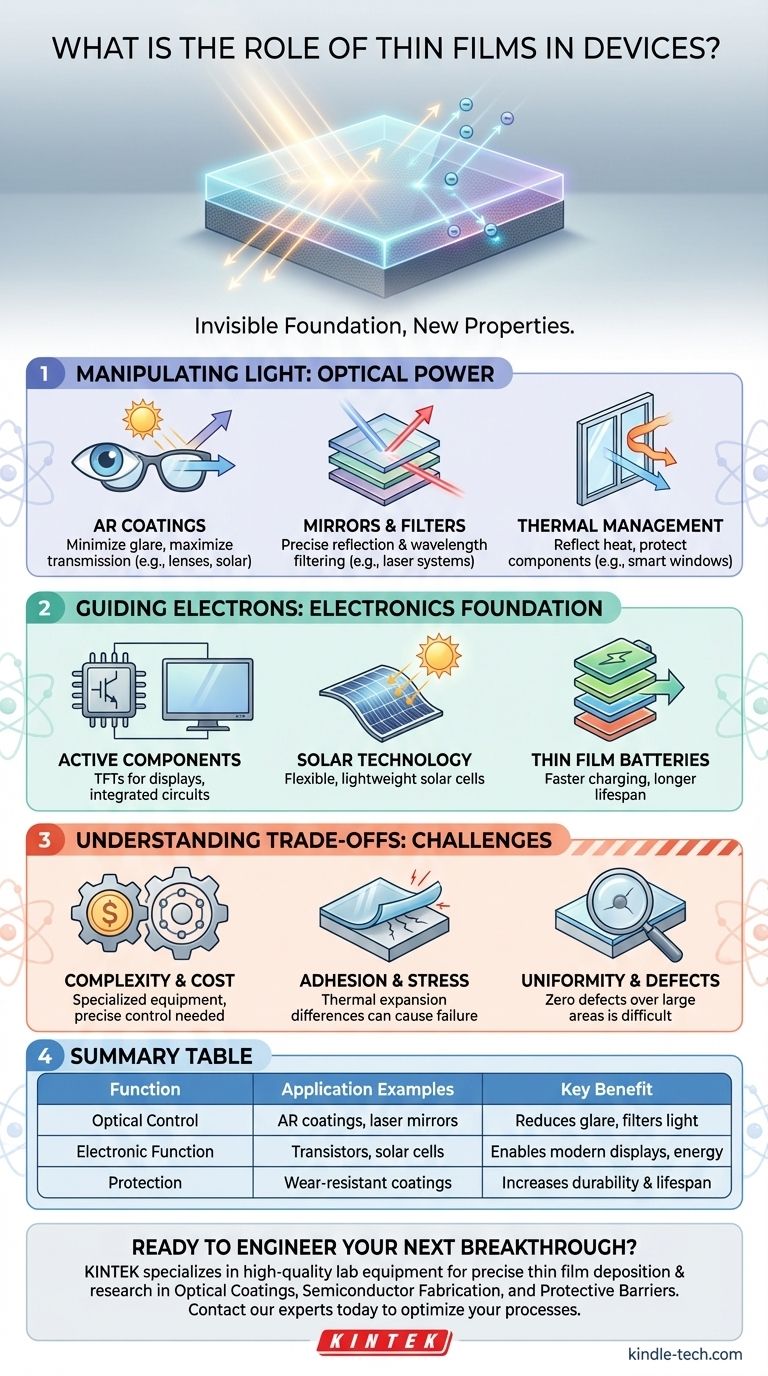
At its most fundamental level, the role of a thin film is to apply a microscopic layer of material to a surface, granting that surface entirely new properties it would not otherwise possess. These engineered layers are the invisible foundation of modern technology, enabling everything from the anti-reflection coating on your glasses to the complex circuitry inside your smartphone and the efficiency of solar panels.
The core function of a thin film is not merely to coat a surface, but to precisely engineer how that surface interacts with light, electricity, heat, or the physical environment. This control at the atomic scale is what enables the performance and functionality of countless modern devices.
Manipulating Light: The Optical Power of Thin Films
Much of thin film technology is dedicated to controlling the flow of light. By depositing one or more layers of specific materials, we can dictate exactly which wavelengths are reflected, transmitted, or absorbed.
Enhancing Transmission and Efficiency
Anti-reflective (AR) coatings are a primary example. They are used on everything from camera lenses and eyeglasses to solar panels and electronic displays.
These coatings are precisely engineered layers that reduce natural reflection, minimizing glare and maximizing the amount of light that passes through the surface. This directly improves the efficiency of a solar cell or the clarity of a display.
Controlling Reflection and Filtering
Thin films are essential for creating highly specialized mirrors and filters. For instance, high-powered laser systems use distributed Bragg reflectors—stacks of alternating thin films—to create mirrors that are nearly 100% reflective for a specific wavelength.
Similarly, by layering different materials, engineers can create notch filters that block a very narrow band of light or coatings on architectural glass that reflect infrared heat while allowing visible light to pass through.
Managing Thermal Energy
Thin films also play a crucial role in managing heat. Infrared-reflecting coatings are deposited inside filament lamps to reflect heat back onto the filament, increasing its brightness and efficiency.
In data storage devices or window panes, specific thin films act as thermal barriers, protecting sensitive components from temperature spikes or preventing heat from entering a building.
Guiding Electrons: The Foundation of Modern Electronics
The entire semiconductor industry is built upon the precise deposition of thin films. The microscopic transistors and pathways inside an integrated circuit are constructed by layering conductive, insulating, and semiconducting films.
Building Active Components
Thin film transistors (TFTs) are the backbone of modern flat-panel displays, including LCD and OLED screens. Each pixel in the display is controlled by its own tiny transistor made from deposited thin films.
This same principle enables the creation of thin film solar cells and batteries, which offer benefits like flexibility, lower weight, and improved energy efficiency.
Enabling New Energy Technologies
Thin film technologies are driving progress in renewable energy and storage. Thin film solar cells can be produced on flexible substrates, opening up new applications where traditional silicon panels are impractical.
Likewise, thin film batteries promise faster charging speeds and longer lifespans, which are critical for everything from consumer electronics to electric vehicles.
Understanding the Trade-offs
While incredibly powerful, implementing thin film technology is not without its challenges. The process of depositing these layers is a highly specialized field of materials science.
Complexity and Cost
Thin film deposition often requires sophisticated equipment, such as vacuum chambers, and extreme precision to control layer thickness, sometimes down to a single layer of atoms. This makes the manufacturing process complex and potentially expensive.
Material Adhesion and Stress
A common failure point is the adhesion between the thin film and the substrate it's applied to. Differences in thermal expansion or internal stress can cause the film to crack, peel, or delaminate, rendering the device useless.
Uniformity and Defects
Achieving a perfectly uniform film with zero defects over a large area is exceptionally difficult. A single microscopic pinhole or impurity in a protective coating can compromise the entire barrier, and non-uniformity in an optical coating can ruin its performance.
Making the Right Choice for Your Goal
The right thin film strategy depends entirely on the functional property you need to engineer.
- If your primary focus is optical performance: Utilize stacked layers of dielectric or metallic films to precisely control the reflection, transmission, and absorption of specific light wavelengths.
- If your primary focus is electronic functionality: Concentrate on depositing and patterning semiconductor, conductor, and insulator films to build active components like transistors or energy devices.
- If your primary focus is mechanical or chemical protection: Prioritize hard, inert materials like specific ceramics or metals to create a durable barrier against wear, corrosion, and other environmental factors.
By understanding that thin films are a tool for fundamentally engineering material properties, you can unlock new performance and possibilities in nearly any technical domain.
Summary Table:
| Function | Application Examples | Key Benefit |
|---|---|---|
| Optical Control | Anti-reflective coatings, laser mirrors, thermal windows | Reduces glare, filters light, manages heat |
| Electronic Function | Transistors (TFTs), integrated circuits, solar cells | Enables modern displays, computing, and energy generation |
| Mechanical/Chemical Protection | Wear-resistant coatings, corrosion barriers | Increases durability and lifespan of components |
Ready to Engineer Your Next Breakthrough with Thin Films?
Thin films are the key to unlocking superior performance in your devices, whether you're developing advanced optics, next-generation electronics, or efficient energy solutions. At KINTEK, we specialize in providing the high-quality lab equipment and consumables needed for precise thin film deposition and research.
Our expertise supports your innovation in:
- Optical Coatings: Achieve precise control over light transmission and reflection.
- Semiconductor Fabrication: Build reliable electronic components with uniform layers.
- Protective Barriers: Enhance product durability with robust, adherent films.
Let KINTEK be your partner in materials science. Contact our experts today to discuss how our solutions can help you optimize your thin film processes and bring your most advanced ideas to life.
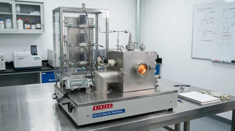
Visual Guide
Related Products
- Aluminized Ceramic Evaporation Boat for Thin Film Deposition
- Tungsten Evaporation Boat for Thin Film Deposition
- Electron Beam Evaporation Coating Oxygen-Free Copper Crucible and Evaporation Boat
- Molybdenum Tungsten Tantalum Evaporation Boat for High Temperature Applications
- Aluminum-Plastic Flexible Packaging Film for Lithium Battery Packaging
People Also Ask
- What is the chemical method for thin film deposition? Build Films from the Molecular Level Up
- Why is an alumina boat selected for catalyst precursors? Ensure Sample Purity at 1000 °C
- What are thin films deposited by evaporation? A Guide to High-Purity Coating
- What is thin film deposition? Unlock Advanced Surface Engineering for Your Materials
- What are the alternatives to sputtering? Choose the Right Thin Film Deposition Method


